
Content last revised on September 20, 2026
6MBP100RTC060-01 Circuit Protection & Reliability: Calibrating Four-Quadrant Power Flow Topologies for Grid Systems
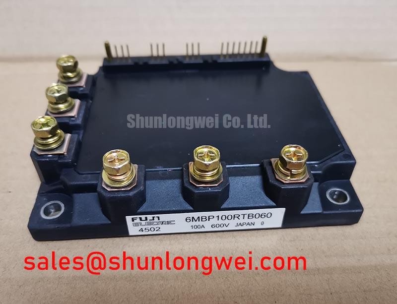
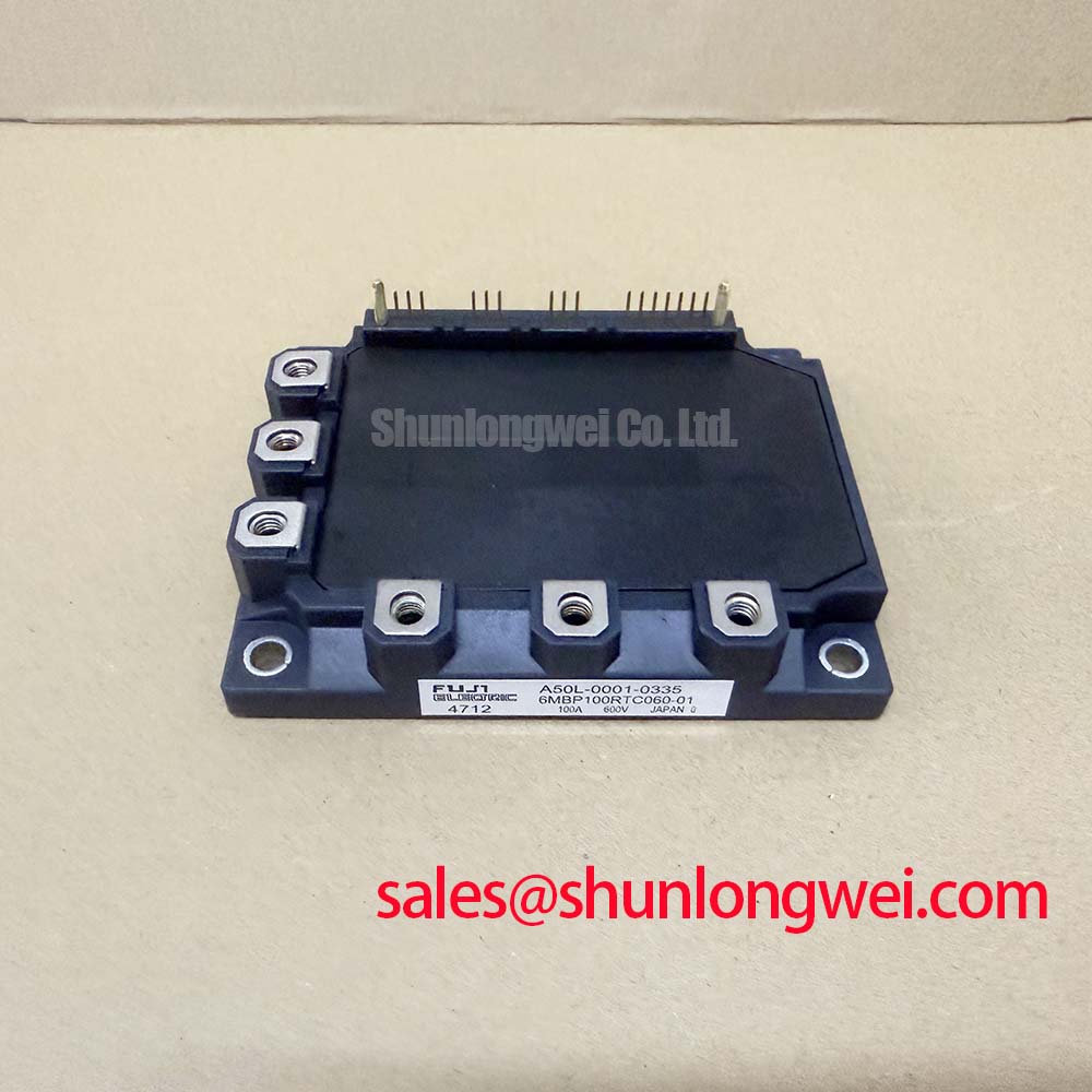
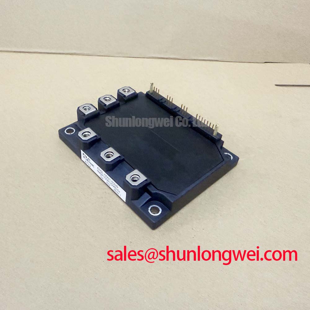
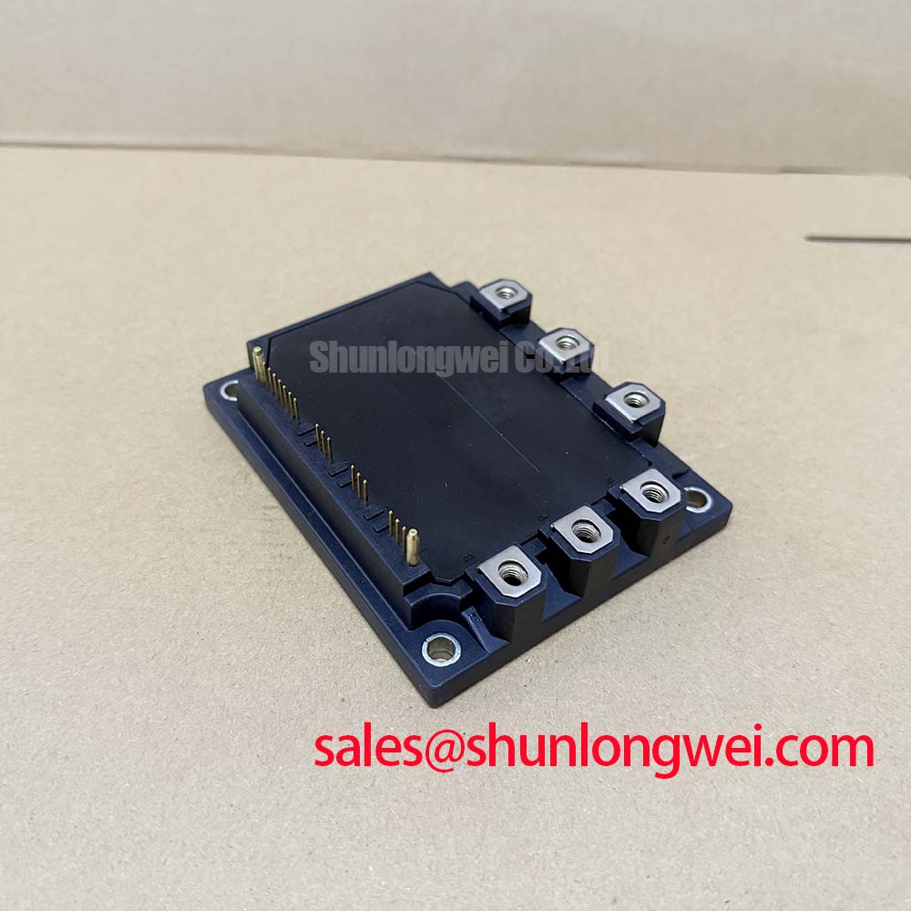
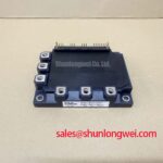
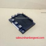
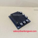
With the DC link discharged and isolated, first inspect the 6MBP100RTC060-01 power terminals for heat discoloration, loose hardware, cracked encapsulation, or conductive contamination, then compare cold-state terminal readings with a known serviceable inverter assembly before applying power.
The Fuji Electric 6MBP100RTC060-01 IGBT module is specified for power conversion equipment requiring a 600 V collector-emitter voltage and 100 A continuous collector current at Tc = 80 °C. Its official maximum collector-emitter saturation voltage is 2.8 V at Ic = 100 A and Vge = 15 V. These ratings establish the electrical identity that must be checked against the removed module and the equipment circuit documentation.
| Official Datasheet Specification | Condition | Value |
|---|---|---|
| Collector-emitter voltage, Vces | Official rating | 600 V |
| Continuous collector current, Ic | Tc = 80 °C | 100 A |
| Collector-emitter saturation voltage, Vce(sat) | Ic = 100 A, Vge = 15 V | 2.8 V maximum |
| Maximum specified junction temperature, Tj | Official rating | +150 °C |
| Thermal resistance, Rth(j-c) | IGBT inverter section | 0.24 °C/W |
In commercial string inverter and micro-grid energy-storage service, a bidirectional converter can move energy between battery racks and the DC link in either direction. The module therefore needs to be evaluated against the actual switching sequence, load-current direction, driver logic, protection response, and thermal condition of the original assembly. The 600 V Vces rating and 100 A Ic rating are official datasheet specifications, not a declaration of suitability for every DC-bus level, switching frequency, battery voltage window, or grid-connected topology.
For a repair assessment, start by verifying that the removed part number, terminal arrangement, control-board connection, heatsink interface, and protection architecture match the replacement position. Check whether the failure occurred during battery discharge, battery charge, grid transfer, or startup. A module damaged during one operating state can leave clues elsewhere in the system, including gate-drive supplies, current sensors, precharge contactors, DC-link capacitors, MOV devices, and the driver board’s fault latch circuit.
Design Consideration: cyclic peak-shaving operation can create repeated temperature changes in the power stage even where average output current appears moderate. The maximum specified +150 °C junction temperature defines a device limit, while the resulting junction temperature in installed equipment depends on current waveform, conduction loss, switching loss, heatsink condition, thermal-interface quality, ambient temperature, airflow, and control strategy. Engineers should verify actual case and heatsink temperatures under the equipment’s own duty profile rather than infer junction margin from the nameplate current alone.
Where multiple current paths are paralleled at system level, static current sharing and switching-time sharing both require measurement. Positive temperature-coefficient behavior can assist current redistribution under some operating conditions, but it does not remove the need to compare gate-drive paths, power-loop symmetry, current-sense calibration, and timing. A current imbalance may indicate unequal interconnect resistance, inconsistent drive behavior, or an issue upstream of the module. Use captured waveforms and a known-good channel as the comparison basis.
⚠️ Field Alert: Disconnect all stored-energy sources and confirm DC-link discharge before loosening module terminals or unplugging driver connections.
Clearance and creepage across exposed busbars, mounting surfaces, and control connections should remain consistent with the original insulation layout and the equipment’s applicable safety design. Do not move sensing wires or driver cables merely to make routing easier; their placement can influence noise coupling and protection behavior. Fuji Electric’s Power Semiconductors Portal provides broader manufacturer product-family context for power-module integration.
Field Diagnostics & Commissioning: Altitude and Radiation Considerations in 6MBP100RTC060-01 Topologies
Before recommissioning a repaired string inverter or energy-storage converter, inspect the installation environment as well as the module. High-altitude sites can change external insulation conditions and system thermal behavior. Terrestrial neutron exposure is also a recognized reliability topic for high-voltage semiconductor systems. No official FIT rate, single-event burnout rate, altitude derating curve, or lifetime prediction is provided here for the 6MBP100RTC060-01; a specific reliability conclusion would require applicable manufacturer data and the complete system voltage and environmental profile.
Design Consideration: when the equipment operates at elevated altitude or with a DC-bus voltage close to its intended operating boundary, the system engineer should validate voltage transients, insulation coordination, cooling performance, and protection reaction under the real site conditions. The correct review is not a generic derating percentage. It is a measured comparison of the observed switching peaks and environmental constraints against the limits documented for the complete inverter assembly.
Commissioning should include a controlled check of gate-drive supply integrity, fault indication, and the high-side drive method used by the original board. Bootstrap capacitor selection cannot be calculated from the published module data above because gate charge and driver quiescent current are not specified in the provided official parameters. Engineering calculation requires the actual driver documentation, switching frequency, required high-side on-time, gate charge at the selected operating point, and leakage paths. Reusing the original validated driver-board component values is generally the safer repair approach unless the board documentation directs otherwise.
If a module has failed, do not assume an isolated semiconductor event. Inspect the gate-drive isolation barrier, optical or digital-isolator supply rails, local decoupling condition, and common-mode noise path. A driver output that appears correct with no DC link applied can still behave differently during switching. Verify gate and collector-emitter waveforms with appropriately rated isolated measurement equipment while following the equipment’s safe test procedure.
For structured checks of terminal condition, waveform capture, thermal observations, and fault isolation, consult the Field Engineer’s Handbook during the repair record process.
Benchtop Waveform Tuning: Mitigating Stress via High-Speed Fault Management and VCE Desaturation
Desaturation protection is normally evaluated as part of the complete gate-driver circuit, not as a standalone characteristic of the IGBT module. During a suspected overload or short-circuit event, the driver must recognize abnormal collector-emitter behavior and remove gate drive in a controlled way. The permissible detection interval, short-circuit withstand capability, and turn-off profile must be taken from the relevant module and driver documentation. The supplied official parameters do not state a short-circuit safe-operating-area duration, so no fixed microsecond protection setting should be assigned to this model on this page.
Engineering Recommendation: preserve the original fault-management concept during a module replacement. If the board uses staged or soft turn-off, confirm that its gate resistor network, desaturation sensing path, fault latch, isolation stage, and local power supply remain electrically intact. Replacing only the power module while overlooking a damaged driver output can produce an immediate repeat failure when the DC link is energized.
On a controlled bench setup, compare turn-on and turn-off waveforms between equivalent phases or against a verified reference assembly. Excess ringing, an unexpected collector-emitter overshoot, delayed gate discharge, or irregular fault timing may indicate parasitic inductance, degraded local capacitors, driver-board damage, probing error, or connection problems. It should not be assigned to one cause without measured evidence.
The 2.8 V maximum Vce(sat) specification at the stated test condition is useful as an official electrical boundary, but it is not a field pass or fail voltage for an unpowered multimeter test. Cold-state diode checks and resistance checks can reveal obvious abnormal conduction paths, yet a dynamic defect may only become visible during controlled switching evaluation. Keep test methods aligned with the equipment service manual and available safety procedures.
For repair teams comparing documented electrical and mechanical compatibility within the same product family, the 6MBI100L-060 can be reviewed as a separate Fuji Electric module reference. Its suitability must be determined from its own official specifications, circuit function, package interface, driver requirements, and original equipment documentation.
6MBP100RTC060-01 Thermal-Electrical Optimization: DC-Bus Low-Inductance Laminated Busbar Practical Tuning
At turn-off, the collector-emitter peak is influenced by DC-link voltage, current-change rate, and inductance in the commutation loop. In practical terms, reducing loop inductance helps suppress inductive overshoot, but the required geometry and acceptable peak margin are system-determined and must be verified with switching tests. No specific busbar-inductance target or snubber value should be assigned without the inverter’s measured waveform data.
Inspect the laminated busbar or equivalent DC-link connection for distortion, loose fasteners, oxidized contact surfaces, displaced insulation films, and unequal conductor spacing. Confirm that the local DC-link capacitors remain physically close to the commutation path as intended by the original design. MOV devices and snubber networks should be checked as coordinated parts of the overvoltage-control system; their presence does not prove that they remain functional after a severe transient event.
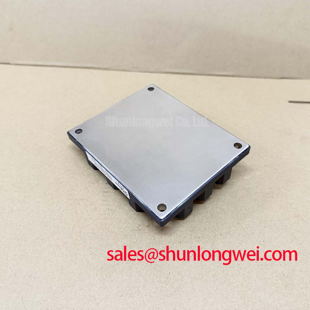
The official inverter-section thermal resistance of 0.24 °C/W Rth(j-c) describes junction-to-case thermal resistance under the manufacturer’s defined conditions. It does not include thermal grease, mounting pressure, heatsink resistance, forced-air performance, or enclosure temperature. During reassembly, clean both contact surfaces, apply the thermal interface material uniformly according to the equipment procedure, and tighten mounting hardware using the original mechanical specification.
After repair, observe temperature progression, fault history, DC-link ripple, and switching-waveform behavior during a controlled load increase. This identifies whether the replacement module is operating within the original system’s intended electrical and thermal environment. For manufacturer background on power semiconductor technologies, refer to Fuji Electric Global Power Semiconductor Technologies.