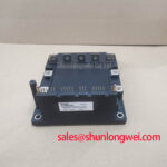
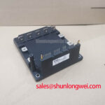
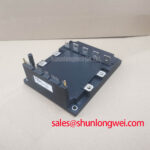
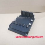
Content last revised on September 21, 2026
Assembly Integrity & Layout Architecture: Implementing Dynamic Braking Chopper Operation for 6MBP150RS060
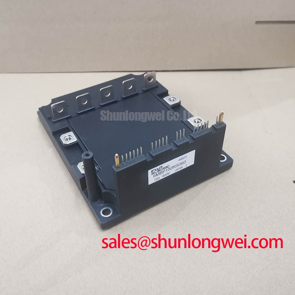
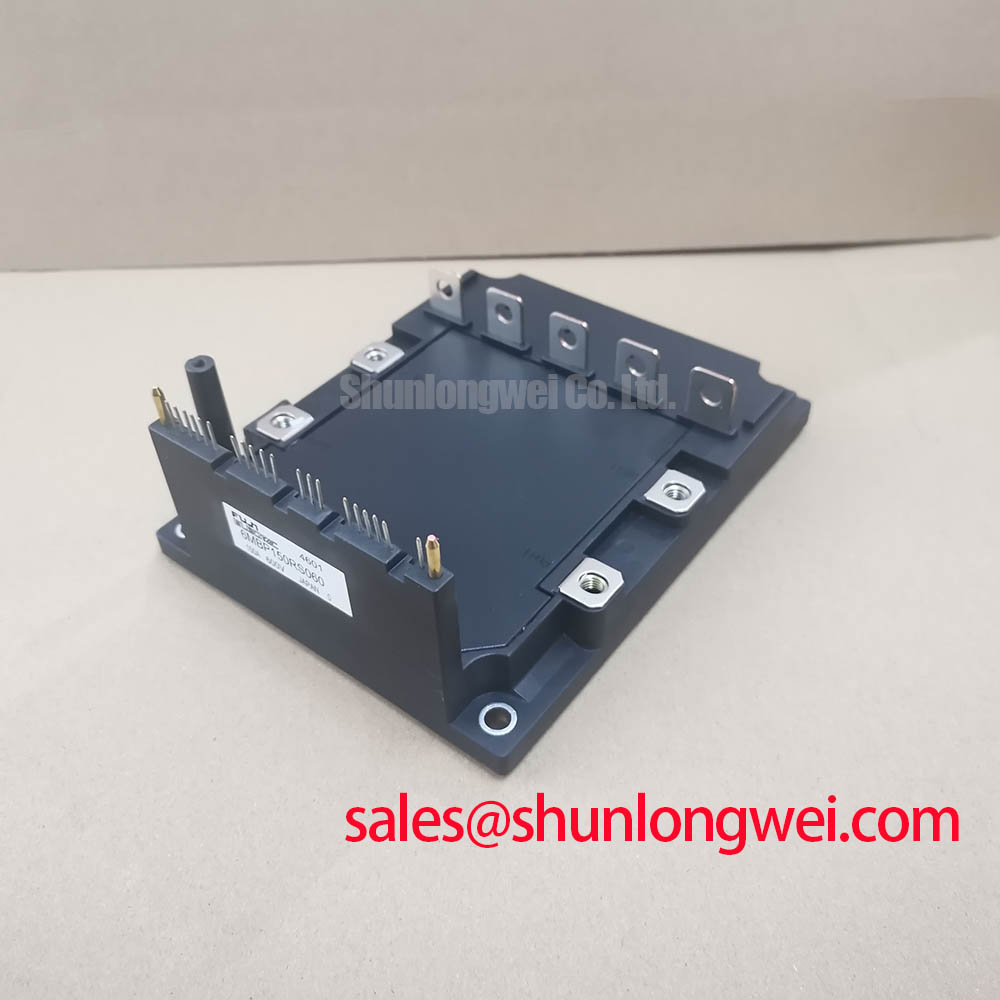
During a stopped-drive repair, inspect the DC bus capacitors, braking resistor terminals, contactors, and cable lugs before attributing a bus overvoltage trip to the power module. A dynamic braking chopper transfers regenerative motor energy from the DC link into a ballast resistor, but the availability and allocation of a chopper switch must be verified from the equipment schematic. The supplied official data identifies the 6MBP150RS060 as a 600V, 150A Fuji Electric module; it does not independently establish a braking-chopper rating or resistor specification.
As a Design Consideration, the braking resistor, switching device, wiring path, and enclosure airflow should be assessed together because deceleration energy can stress each part of the energy path. Check for heat discoloration at resistor connections, loosened busbar joints, cracked insulators, and signs that a conductor has moved under vibration. A chopper fault may coexist with weak DC-link capacitance, incorrect voltage sensing, a drive-command issue, or an external mechanical load returning energy to the bus.
Keep the chopper current path compact where the original layout permits, with adequate clearance appropriate to the equipment’s working voltage, contamination level, and applicable installation rules. System engineers should confirm DC-link peak voltage during controlled switching tests rather than infer safe headroom from the module rating alone. For comparison during an equipment review, the 6MBI100L-060 is a related 600V module reference, though current capability, package interface, control arrangement, and thermal path require separate verification.
⚠️ Field Alert: Do not tighten live-busbar hardware or reconnect control cables until the DC link has been discharged and its residual voltage has been measured safely.
Benchtop Waveform Tuning: Mitigating Stress via Suppressing Cres-Induced Gate-Voltage Spikes on 6MBP150RS060
Before applying control power, compare every power and control connection with the original module drawing and the host board’s connector map. Do not assume that physically similar module families share the same terminal arrangement, signal assignment, or protection interface. The relevant Fuji Electric product context can be reviewed through the Fuji Electric Power Semiconductor and IPM Modules resource.
High switching-voltage slew rate can couple through device capacitances and wiring parasitics, causing a non-commanded gate-voltage rise in the opposite switch position. In a bridge circuit, that condition can contribute to cross-conduction if the driver return path, turn-off impedance, timing control, or clamp behavior is unsuitable. A Design Consideration is to use the driver architecture specified by the original system, including its active Miller-clamp function where provided, and verify turn-off behavior with isolated measurement equipment.
Negative gate bias is sometimes used in industrial gate-drive designs to improve turn-off immunity, but its required value must be taken from the original drive specification and verified against the applicable Fuji Electric documentation. It must not be selected from a generic range. Inspect the gate-drive board for damaged clamp components, degraded isolated supplies, connector fretting, and altered resistor values. Oscilloscope traces should be compared with a known-good channel or validated design target while checking switching-node voltage, commanded gate signal, and the local driver return.
Busbar fastening also matters. A loose laminated bus assembly or unsupported cable can alter loop geometry under vibration and make ringing harder to reproduce on the bench. Secure conductors according to the equipment manufacturer’s mechanical instructions and confirm that creepage and clearance remain intact after assembly.
Benchtop Waveform Tuning: Mitigating Stress via Auxiliary Emitter Return Trace Separation on 6MBP150RS060
When a repaired unit shows irregular switching noise, first separate a control-loop problem from a power-loop problem. The high-current emitter return can develop a voltage during switching; if the driver reference shares too much of that path, the apparent gate voltage at the device can differ from the gate voltage measured at the driver output. This can produce unstable turn-off behavior, false protection activity, or waveform variation between otherwise similar legs.
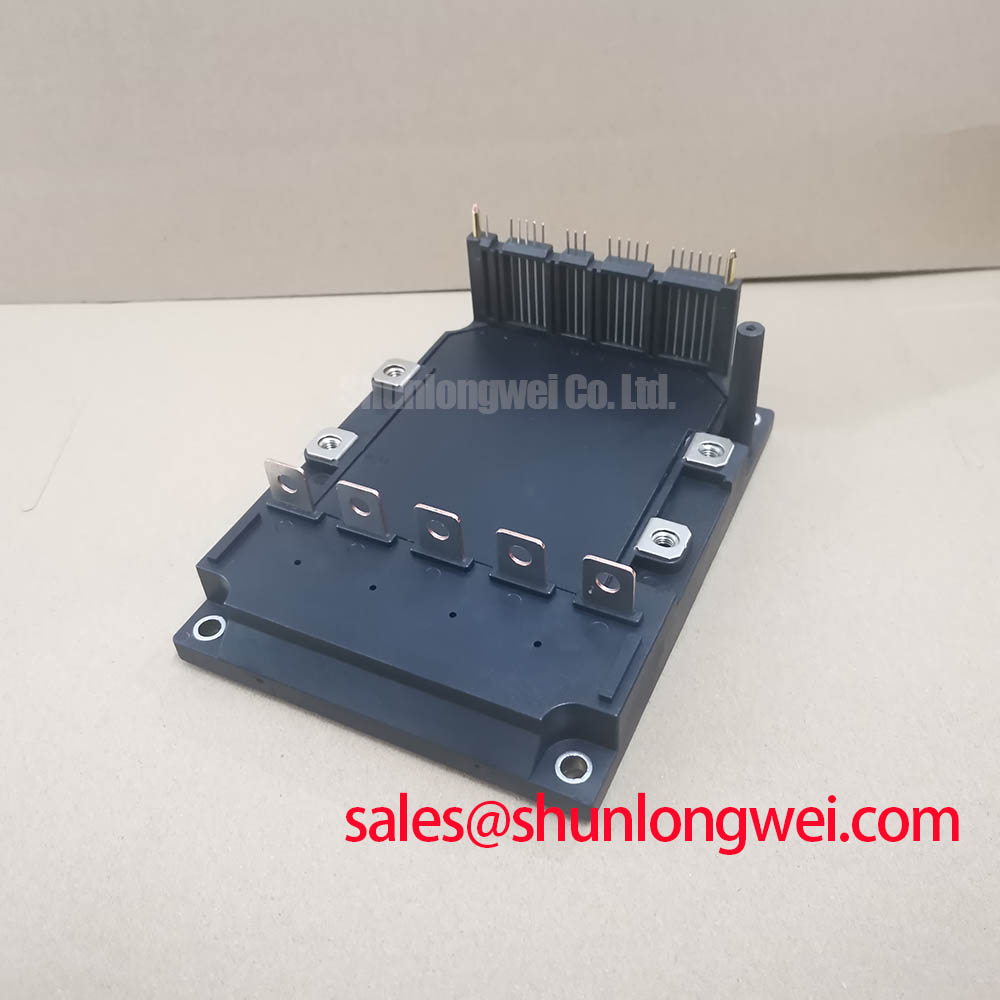
As an Engineering Recommendation, preserve the original distinction between the gate-driver return and the main high-current return wherever the module and control board interface supports it. The system integrator should verify the actual auxiliary-emitter or control-reference connection from the original module documentation rather than infer it from package appearance. Avoid routing a sensitive driver return alongside a high-current busbar when servicing or replacing harnesses.
Check that the controller’s dead-time setting is retained after board replacement or parameter restoration. Dead time is system-determined: it must accommodate the actual switching transition, driver delay, current direction, temperature condition, and measured ringing. Excessively short timing can permit overlap, while unnecessarily long timing can affect output behavior. Measure at the relevant operating point before changing firmware or gate-drive components.
For broader integration principles covering gate-drive loops, thermal interfaces, and switching topologies, see IGBT Design & Integration. This is engineering background rather than an official performance guarantee for this specific module.
6MBP150RS060 Circuit Protection & Reliability: Assessing Atmospheric Neutron Radiation Effects
Do not assign a numerical neutron-induced failure rate, altitude derating factor, or Single Event Burnout prediction to the 6MBP150RS060 without a model-specific manufacturer qualification source or an applicable validated study. The official structured information available here confirms 600V and 150A ratings, but it does not provide a FIT figure, an altitude operating limit, or a cosmic-radiation qualification claim.
At elevated installation sites, atmospheric neutron exposure is a Design Consideration that should be assessed by the equipment owner using the actual DC-bus condition, switching transients, enclosure environment, mission profile, and applicable reliability requirements. The practical service task is to confirm that transient suppression, DC-bus sensing, overcurrent response, and cooling performance continue to operate as intended. A repeated protection event should be investigated through recorded bus voltage, current feedback, thermal signals, and gate-drive waveforms rather than assigned to one cause without evidence.
For manufacturer-level module-family information, consult the Fuji Electric Power Semiconductors Portal. Any environmental qualification decision should be based on the specific equipment duty and documented technical evidence.