

Content last revised on October 28, 2026
6MBP200RA120 Circuit Protection & Reliability: Calibrating Terminal Heating Prevention Through Periodic Inspection
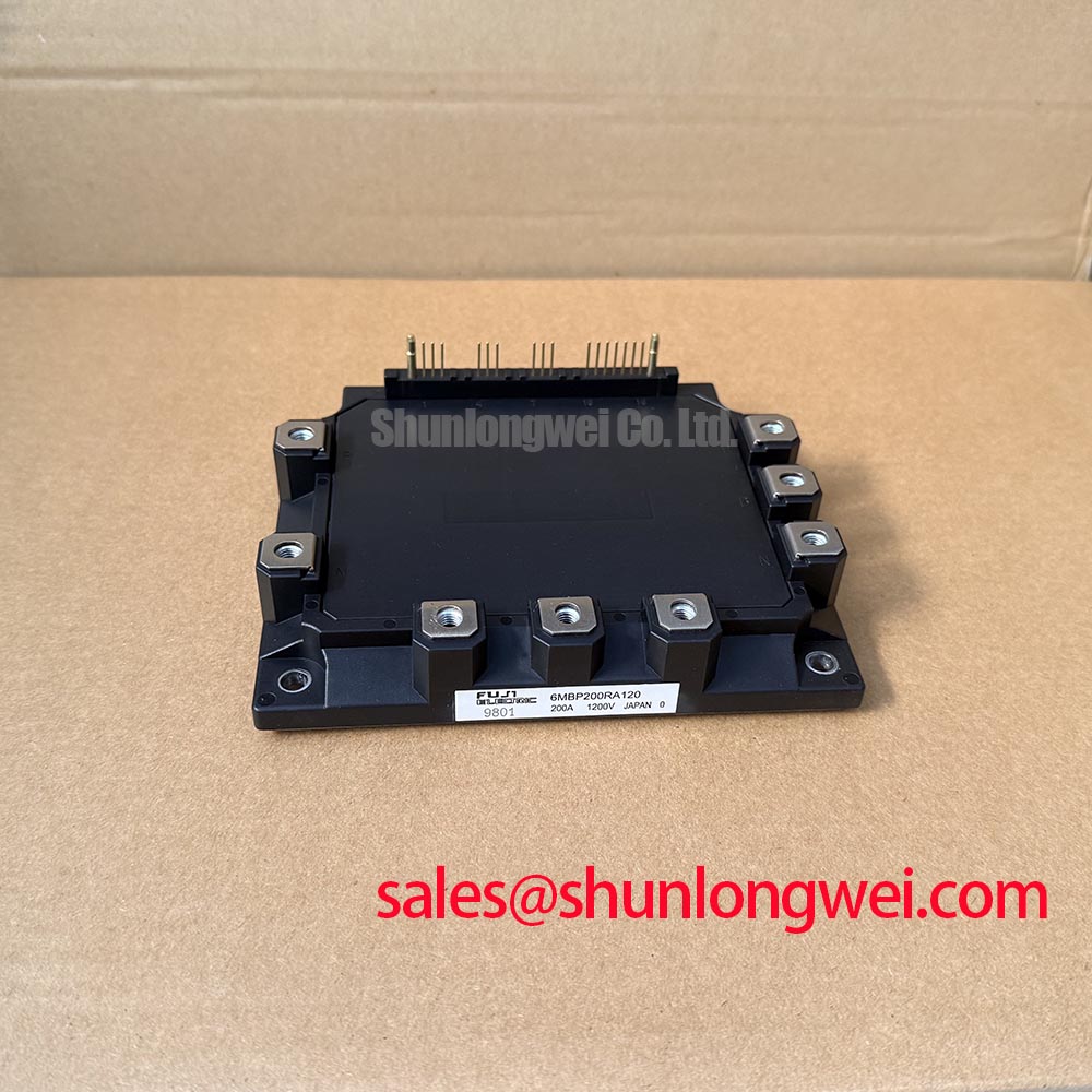
Terminal heating is best controlled by treating the bolted power connection as part of the electrical circuit, not as a purely mechanical fastening point. During a maintenance interval, isolate and discharge the equipment according to the site safety procedure, remove parallel current paths where practical, and use a four-wire micro-ohmmeter to assess the contact resistance of each high-current terminal. A low, repeatable resistance target may be used for this service procedure, but the acceptance limit should be aligned with the equipment manufacturer's maintenance standard, conductor arrangement, and instrument uncertainty.
Record the measurement position, probe force, ambient condition, and terminal hardware condition. A single reading can be misleading when oxide films, uneven washers, plated surfaces, or probe placement alter the contact interface. Repeat the measurement from equivalent points on each phase and compare the results with the known-good phases of the same converter. A rising value across service intervals deserves attention even when the module remains electrically functional, because additional joint resistance converts load current into localized heat.
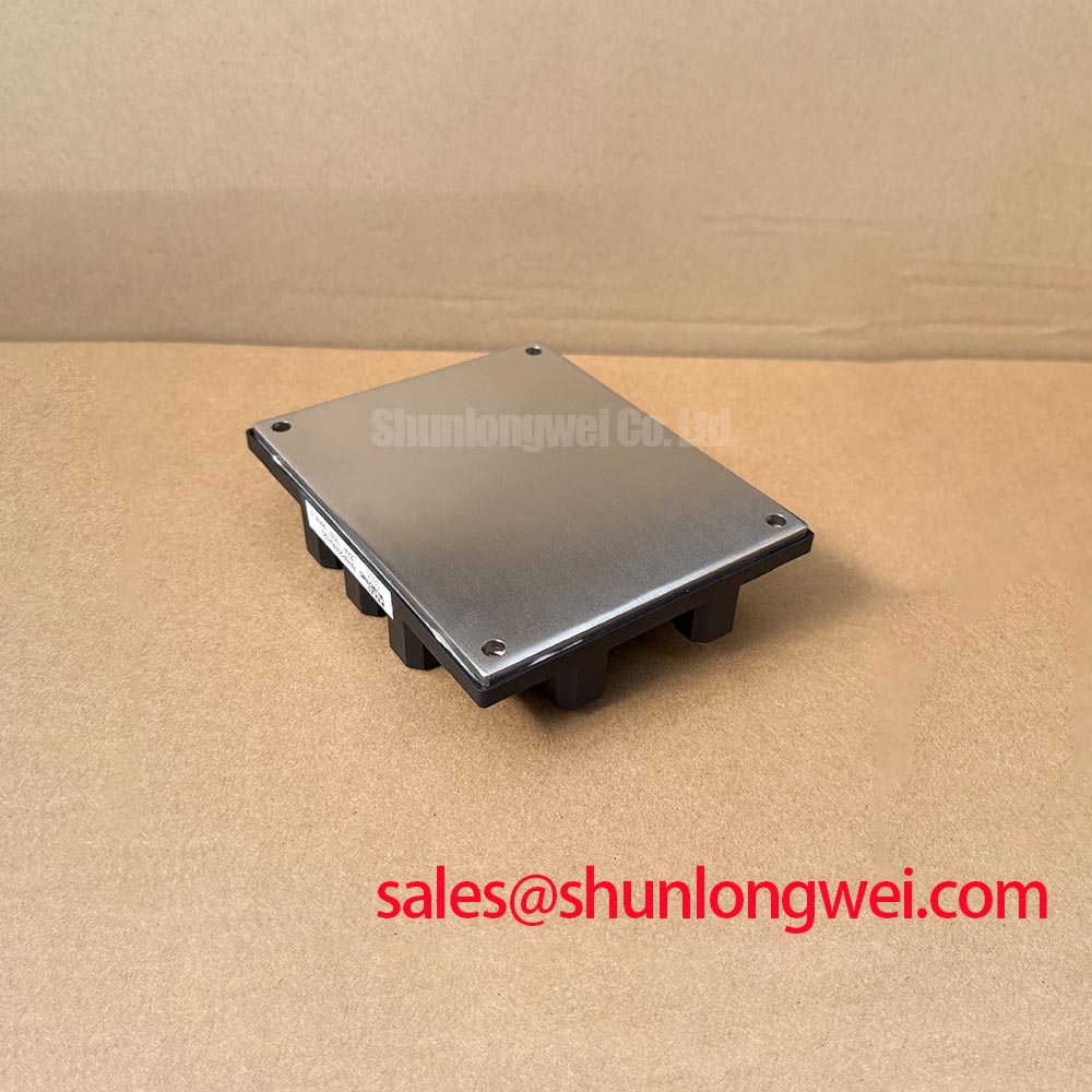
Thermographic inspection should be performed after the converter has reached a stable operating condition representative of the intended duty. Use the same emissivity treatment and viewing angle for comparable terminals, and keep the camera perpendicular enough to reduce reflection errors from bright metal surfaces. Look for phase-to-phase temperature imbalance, a concentrated hot spot at the lug or busbar interface, and heat spreading toward the module terminal. The thermal pattern should be reviewed alongside current sharing, ambient temperature, airflow, and the cooling assembly rather than treated as a standalone failure verdict.
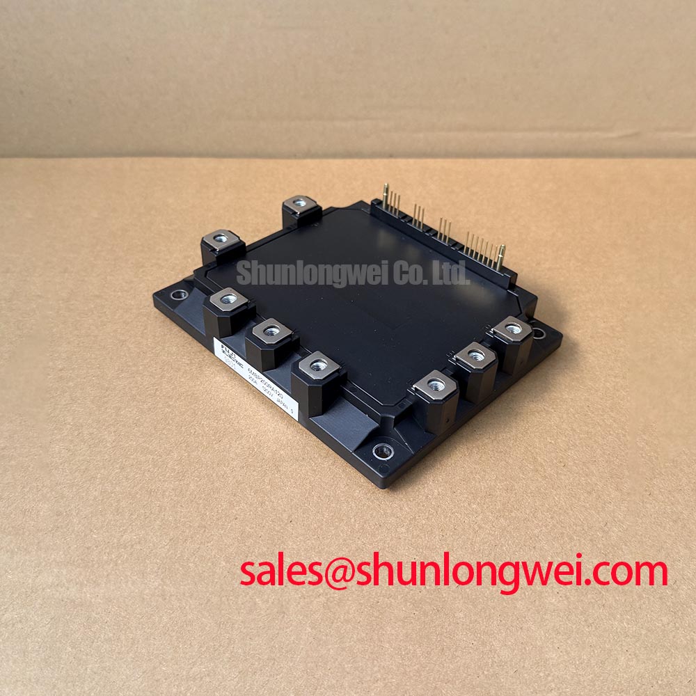
Mechanical alignment matters when the module is installed on a busbar assembly. The conductor should meet the terminal without forcing the module body, and the fastening sequence should not twist the terminal or lift one edge of the contact surface. Keep power conductors short and appropriately supported so that vibration and cable weight do not repeatedly load the terminal joint. Clearance around the live bus structure must also be maintained according to the applicable insulation coordination and equipment standard; the module's voltage rating alone does not define the finished assembly's clearance or creepage requirement.
Protection coordination begins upstream and continues through the gate-drive and control boards. A semiconductor fuse should be selected by comparing its clearing characteristic and I²t behavior with the converter's prospective fault current, the module's permitted surge conditions, and the DC-link capacitor energy. The fuse cannot be evaluated only by its nominal current label. Check whether its interruption behavior allows the protection circuit to act before the module experiences destructive short-circuit stress, while also avoiding nuisance operation during controlled inrush, regeneration, or capacitor charging.
For the front-end or active rectifier portion of an energy-storage converter, a related device such as 6MBP150TEA060 may appear in a complementary topology review. It should be treated as a separate component evaluation rather than an automatic substitute. Confirm voltage class, current class, internal circuit configuration, terminal assignment, driver requirements, and thermal conditions for the specific design.
6MBP200RA120 Operational Boundaries: Evaluating Auxiliary Emitter Return Trace Separation Limits
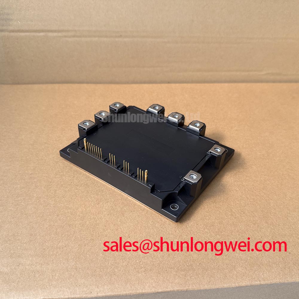
Separate the auxiliary emitter return used by the gate driver from the main high-current emitter path before attempting to tune switching behavior. The driver reference should return through the intended low-impedance control path, while the power-current return should follow the main commutation path. When these routes share copper or a narrow via transition, the voltage developed by power-current slew can appear directly at the driver reference. The resulting apparent gate disturbance may be mistaken for a gate-resistor problem even when the resistor value is unchanged.
Use a compact gate-drive loop with controlled routing from the driver output to the module gate and from the auxiliary emitter return back to the driver reference. Minimize the area enclosed by the drive loop, keep the return physically close to the outgoing gate path, and avoid routing the control return alongside a high di/dt collector or emitter conductor for an extended distance. The final arrangement must be verified with the actual module, driver, busbar, and DC-link capacitor because the interaction is determined by the complete commutation loop.
Gate-loop parasitic inductance can produce ringing during both turn-on and turn-off. A practical commissioning sequence is to inspect the gate-to-emitter waveform directly at the module terminals with a measurement setup that does not introduce a long ground lead. Compare the waveform at light load and rated operating conditions, then examine whether the disturbance is synchronized with the opposite switch transition. Oscillation that changes with probe placement may be a measurement artifact; oscillation that tracks the switching edge and appears on the control return should prompt a layout and reference-path review.
💡 Pro Tip: Keep the auxiliary emitter return physically independent from the main power emitter route and validate the final busbar symmetry with a properly isolated oscilloscope during double-pulse and full-load switching tests.
Gate resistance is a tuning element, not a universal cure. Increasing damping can reduce ringing but may increase switching loss, while reducing it can sharpen transitions and increase overshoot or electromagnetic coupling. Select the starting point from the gate-driver design and tune it against measured gate voltage, collector-emitter voltage, current commutation, device temperature, and protection response. A driver with separate turn-on and turn-off paths may require independent assessment of each transition.
The driver supply also needs attention during repetitive switching. If the control board uses an isolated supply or bootstrap arrangement, inspect the supply recovery during the complete PWM pattern, including low modulation index, high modulation index, regeneration, and fault reset. Bootstrap capacitor charging, diode reverse recovery, driver undervoltage behavior, and pulse-width limitations can interact with the module's switching sequence. The appropriate supply voltage and timing limits are system-design values and should be confirmed from the original driver and inverter documentation.
| Evaluation item | 6MBP200RA120 | Related device for separate review |
|---|---|---|
| Manufacturer | Fuji Electric | Fuji Electric family reference |
| Product category | IPM Module | IPM Module reference |
| Rated voltage | 1200.0 V | Verify from the applicable device documentation |
| Rated current | 200.0 A | Verify from the applicable device documentation |
| Package | Fuji Power Module | Confirm mechanical and terminal compatibility |
| Cross-reference page | Primary evaluation item | 6MBP100RA120 |
The table separates confirmed parameters for the 6MBP200RA120 from information that requires device-specific verification. A lower-current family member may be relevant when the system's continuous and transient current requirements are different, but a replacement decision should include thermal impedance, protection behavior, pin assignment, gate charge, switching loss, and mechanical fit. Do not infer interchangeability from a shared naming pattern.
For technical background on gate-drive routing, thermal paths, and converter topology, consult the IGBT Design & Integration reference. Fuji Electric's semiconductor information can also be reviewed through its Power Semiconductor & IPM Modules resource and the Fuji Electric Europe semiconductor portal.
6MBP200RA120 Operational Boundaries: Evaluating High dv/dt Cross-Conduction Shoot-Through Limits
Investigate cross-conduction by observing both switches in the affected leg at the same time, with attention to gate-to-emitter voltage during the opposite device's high-voltage transition. A high dv/dt event can couple through the Miller capacitance and lift the inactive gate. If the gate driver has insufficient sink capability, excessive common-source inductance, or an exposed return path, the inactive device may receive an unintended turn-on command. The result can be additional current, abnormal switching loss, or a protection event without a simple static resistance fault.
An active Miller clamp can provide a low-impedance path that holds the inactive gate near its intended off-state during the vulnerable interval. The clamp must be placed and routed according to the selected driver architecture, with its return referenced to the same auxiliary emitter point used by the control signal. A negative gate bias may be considered where the driver and module documentation explicitly permit it, but the actual bias value, supply tolerance, transient behavior, and insulation requirements belong to the complete gate-drive design rather than to the module's stated 1200 V and 200 A ratings.
Dead time should be evaluated against actual turn-off delay, gate discharge behavior, temperature, current direction, and the reverse-recovery behavior of the commutating path. Excessive dead time can increase diode conduction and regeneration stress; insufficient dead time can allow overlap during abnormal driver propagation or supply variation. Measure the timing at the module pins rather than relying only on controller register values. Isolated driver propagation mismatch and common-mode transient immunity should be checked across temperature and supply conditions, especially when optocouplers or digital isolators are used on an industrial drive board.
In a string inverter or micro-grid storage converter, regeneration and braking events can change the switching pattern sharply. The DC-link clamp, braking chopper, and high-power braking resistor must be assessed for the energy and pulse profile created by the system. The resistor absorbs energy at the system level, while the switching module still experiences current, voltage, thermal, and commutation stress during each braking event. Verify the chopper control response, resistor thermal recovery, fuse coordination, and DC-link voltage waveform together rather than assigning the entire transient burden to the IPM.
During fault testing, capture gate voltage, collector-emitter voltage, phase current, DC-link voltage, and driver fault feedback on a synchronized time base. Confirm that the protection circuit recognizes the intended fault and that the gate command is removed without creating a secondary turn-on pulse. Short-circuit testing and desaturation response require equipment-specific procedures, controlled energy, suitable probes, and a safe test enclosure. The resulting waveform should be compared with the module and driver operating limits before the converter is returned to service.
Layout separation also supports common-mode transient control. Keep high-voltage switching nodes away from isolated communication traces, feedback references, and gate-driver supply returns. Avoid unnecessary copper overlap between the switching node and the control-side ground plane, and provide a deliberate current path for displacement current. The finished assembly should be tested for control errors, nuisance trips, and gate disturbance under the highest practical switching stress. These checks are particularly relevant when the same power stage serves both maximum-power-point tracking and bidirectional storage operation.
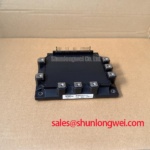
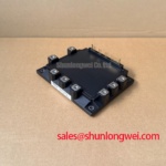
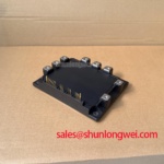
When sourcing a replacement, record the full module marking, terminal arrangement, cooling interface, driver board revision, and converter fault history. The 6MBP200RA120 remains the reference device for the stated 1200.0 V, 200.0 A ratings and Fuji Power Module package; successful integration still depends on matching the electrical, mechanical, thermal, and protection interfaces of the host equipment.