Content last revised on October 12, 2026
6MBP150TEA060 Thermal Electrical Optimization: Screening Substrate Ceramic DBC Micro Crack Practical Tuning
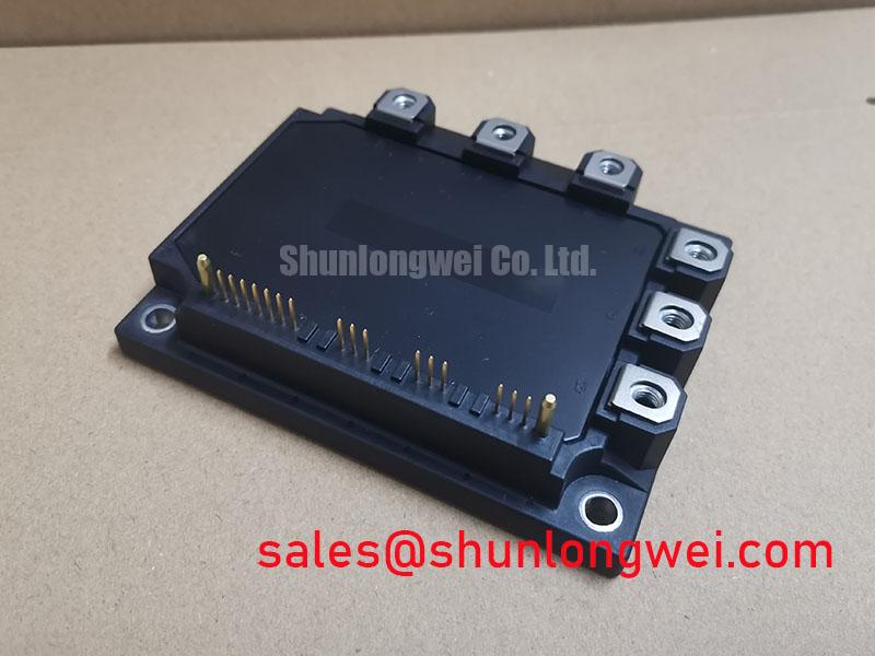
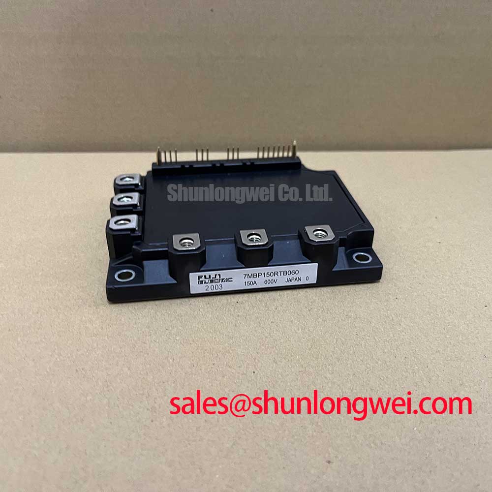
When an inverter welder trips during a high-current cycle, isolate the DC bus, discharge it according to the equipment service procedure, and check the replacement module’s terminal-to-baseplate condition before reconnecting the drive board. The part under evaluation is the 6MBP150TEA060 from Fuji Electric, specified at 600.0 V and 150.0 A in a Fuji Power Module package.
For industrial inverter welders and medium-frequency induction heating supplies, the first compatibility check is not the label alone. Compare the original circuit topology, gate-driver arrangement, cooling interface, protection feedback, and terminal layout with the replacement assembly. The electrical ratings identify the component class, while switching behavior, mechanical contact, and protection coordination determine whether the installed system can operate within its intended limits.
| Manufacturer | Fuji Electric |
| Part number | 6MBP150TEA060 |
| Rated voltage | 600.0 V, Official Specification |
| Rated current | 150.0 A, Official Specification |
| Package | Fuji Power Module, Official Specification |
Begin the insulation assessment by separating the module from the drive circuit and checking terminal-to-baseplate isolation with an appropriate insulation tester. The supplied engineering screening criterion is at least 500 MΩ at 2.5 kV DC; this is a field verification target for assembly integrity, not a substitute for the manufacturer’s complete insulation specification. Apply the test only after confirming that connected gate drivers, sensors, capacitors, and control electronics cannot be exposed to the test voltage.
A low or unstable reading should be treated as evidence requiring further isolation rather than as proof of a ceramic substrate crack. Contamination, conductive dust, moisture films, damaged mounting insulation, incorrect probe placement, or a cable still connected to the power circuit can all influence the result. Repeat the test with the module electrically separated, record the ambient condition, and compare the terminal-to-baseplate reading with phase-to-phase and gate-related checks appropriate to the circuit.
DBC substrate damage is often investigated after a thermal event, excessive mechanical loading, or repeated temperature cycling. Inspect the baseplate and terminal region under suitable lighting for impact marks, distortion, discolouration, lifted hardware, or contamination paths. Do not use visual inspection as the only acceptance method. A clean exterior does not establish the absence of internal ceramic or bonding damage, while a surface deposit can create a measurable leakage path without permanent substrate failure.
Clearance and creepage must be preserved around high-potential terminals, especially where airborne dust from welding operations or metal-processing equipment can accumulate. The final spacing is determined by working voltage, pollution environment, material group, altitude, and the applicable equipment standard. Designers should keep the power path physically separated from control wiring, prevent loose conductive particles from settling near the module, and verify the finished assembly after enclosure installation rather than judging the bare module in isolation.
For equipment exposed to dust, inspect the heatsink pocket, insulating sheet, fastener heads, and cable lugs during service. Any burr, washer deformation, or trapped particle can create local stress or compromise insulation. The Fuji Electric power semiconductor and IPM module reference provides manufacturer-level product context, while the completed equipment still requires application-specific insulation and environmental validation.
Preventing Spurious Faults: Gate Drive Resistance Calibration when Retrofitting 6MBP150TEA060
When a modern power module is fitted to a legacy gate-drive board, calibrate the turn-on and turn-off paths separately instead of treating one resistor value as suitable for both transitions. The external RG(on) and RG(off) influence switching speed, gate ringing, switching loss, Miller coupling, and the stress seen by the driver output. The correct values are system-dependent and should be established through controlled switching tests using the actual DC-link, bus layout, gate wiring, and load condition.
Start by confirming that the driver can supply and remove the required gate charge for the selected switching frequency. A resistor change can alter the driver’s peak current demand and the time spent near the Miller plateau. Observe the gate-to-emitter waveform directly at the module terminals, using a measurement arrangement that minimizes probe-loop inductance. A ringing waveform, unexpected plateau movement, or unequal behavior between parallel channels may indicate a gate-loop impedance or return-path problem rather than a simple resistor tolerance issue.
Turn-off behavior deserves particular attention in retrofit work. Excessive turn-off speed can increase collector-emitter overshoot and radiated interference, while excessive damping can increase switching loss and thermal loading. The engineering objective is to balance these effects while keeping the measured transient within the module and system voltage limits. The final setting should come from waveform evidence, thermal observation, and protection response rather than from copying the resistor fitted to a different module family.
Bootstrap supplies require the same discipline. Size the bootstrap capacitor from the high-side gate-charge requirement, driver quiescent current, charging losses, leakage, switching duty, and the permitted high-side supply ripple. The capacitor must retain adequate gate-drive voltage for the complete high-side conduction interval, including startup and transient operating conditions. A nominal capacitance value alone does not establish reliable operation. Check the driver’s undervoltage-lockout behavior and confirm that the bootstrap diode, resistor, layout, and charging interval support the intended duty cycle.
For an inverter welder, also review the relationship between gate timing and the semiconductor fast fuse. Fuse coordination uses the available short-circuit current, clearing time, and fuse I²t capability in relation to the module’s short-circuit withstand behavior. The fuse is not a replacement for desaturation or overcurrent protection, and a fuse that interrupts the supply eventually may not prevent semiconductor damage during the first fault pulse. Protection timing, gate shutdown, dead-time, and the physical fault loop must be evaluated together.
Where an alternative Fuji module is being considered for a related installation, the 6MBP100RTB060 should be compared through its own voltage, current, terminal, gate-drive, mechanical, and switching specifications. Similar package naming does not establish drop-in compatibility.
6MBP150TEA060 Operational Boundaries: Evaluating and Eliminating Thermal Grease Pump-Out Limits
Check the mating surfaces before applying thermal interface material. Place a straightedge across the heatsink contact area and inspect for bowing, machining marks, embedded particles, and damage around the fastener holes. Examine the module baseplate for burrs or distortion without attempting to flatten it by force. Uneven contact increases local thermal resistance and can concentrate mechanical load on the substrate during tightening.
The interface compound should be applied as a thin, continuous film that fills microscopic surface irregularities without creating thick pockets. A 50 to 80 µm TIM layer is a general engineering starting range, not an official 6MBP150TEA060 specification; the final result depends on the compound, surface finish, pressure distribution, and supplier instructions. Pump-out risk is influenced by repeated thermal expansion, excessive compound thickness, uneven clamping, and relative movement between the baseplate and heatsink.
Use a calibrated torque tool and tighten the fasteners in a diagonal cross-pattern, bringing the baseplate into contact progressively. The applicable torque is determined by the fastener size, thread engagement, washer arrangement, module construction, and manufacturer installation guidance. Do not infer a torque value from the 150 A rating. After tightening, check that the module has not shifted, the terminal hardware remains aligned, and the heatsink has not tilted against the baseplate.
⚡ Field Alert: Disconnect power and verify the DC bus is discharged before touching module terminals, gate wiring, or heatsink fasteners.
In service, investigate rising case temperature alongside airflow, fan performance, heatsink fouling, compound migration, and fastener retention. A dry edge or displaced compound does not by itself prove pump-out, because poor initial spreading and surface contamination can produce a similar pattern. If the assembly is being rebuilt, clean both mating surfaces using a process compatible with the compound and insulation materials, then document the tightening sequence and inspection result.
Thermal design should also account for the switching waveform. Higher turn-on or turn-off loss raises junction temperature even when average output current appears acceptable. The forward drop and switching loss data required for a complete thermal calculation must come from the applicable device documentation and operating condition. Use measured case temperature and the actual cooling arrangement to validate the assembled inverter rather than assigning a fixed thermal limit from the package description alone.
6MBP150TEA060 Circuit Protection and Reliability: Optimizing Gate Drive Loop Geometry
Separate the auxiliary Kelvin emitter return from the main high-current emitter path wherever the module interface and driver topology provide that distinction. The gate driver should reference the emitter at the intended control point, while the power return carries the large commutation current through its own low-impedance path. Shared copper can create emitter mutual coupling, allowing the load-current voltage drop to appear in the gate-drive loop and encouraging oscillation or false turn-on.
Keep the gate path and its return close together, with short conductors and a clearly controlled route back to the driver. Avoid running the gate trace beside high-current collector or emitter conductors for long distances. The commutation loop should be compact to reduce parasitic inductive voltage during rapid current change, but the exact geometry is determined by the module terminals, bus structure, insulation requirements, and switching test results.
During commissioning, monitor gate-to-emitter voltage, collector-emitter voltage, phase current, and driver supply behavior at the same operating point. Look for a gate disturbance during the opposite switch transition, unexpected plateau extension, asymmetric overshoot, or a driver supply dip that coincides with a fault. These observations help distinguish gate-loop coupling from bootstrap weakness, control timing error, load abnormality, or protection miscoordination.
The Miller plateau is governed by the device’s collector-gate charge behavior and the applied gate-drive impedance. A larger effective Cres during a voltage transition can transfer more displacement current into the gate loop, so the layout and turn-off clamp must be assessed together. An active gate clamp may be considered where the driver and module application support it, but its threshold, current capability, timing, and interaction with the negative or zero-voltage gate state must be validated by the system designer.
Reverse recovery from the freewheel diode also affects the commutation event. A diode with softer recovery can reduce the abrupt current transfer that contributes to voltage ringing and EMI, but the resulting recovery energy and switching loss still belong in the thermal and protection assessment. Do not treat a soft recovery factor as a stand-alone compliance claim. Check conducted and radiated behavior at the assembled inverter, with the final enclosure, cabling, busbar, and control harness installed.
For practical measurement methods covering power-module testing, failure analysis, and reliability evaluation, consult the Field Engineer’s Handbook. Fuji Electric’s power semiconductor portal is also a useful manufacturer reference when matching the module family to the original equipment documentation.