Content last revised on September 16, 2026
6MBP30VAA060-50 Thermal-Electrical Optimization: Differential Gate-Source Loop Routing to Practical Tuning
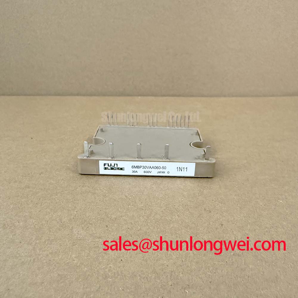
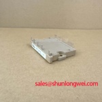
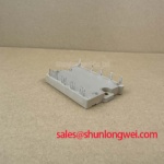
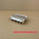
With the drive fully isolated and the DC link discharged, first verify the equipment bill of materials and nameplate requirement against the 6MBP30VAA060-50 electrical limits before reconnecting any control or power wiring. This Fuji Electric IPM module is specified with a 600 V collector-emitter voltage rating, 30 A continuous collector current, and 60 A collector pulse current for 1 ms. These ratings establish the electrical boundary for evaluating a replacement in precision stepper and BLDC servo motion actuator drives, where motor acceleration, regenerative events, switching layout, cooling condition, and control timing must all be assessed as a system.
| Official Specification | Value |
|---|---|
| Manufacturer | Fuji Electric |
| Module Type | Intelligent Power Module |
| Collector-Emitter Voltage, VCES | 600 V |
| Continuous Collector Current, IC | 30 A |
| Pulse Collector Current, ICP | 60 A for 1 ms |
| Collector Power Dissipation per IGBT, PC | 103 W |
| Control Supply Voltage, VCC (absolute maximum) | -0.5 V to 20 V |
| Fault Output Voltage, VFO | VCC |
| Short-Circuit Trip Level | 45 A minimum |
| Over-Temperature Trip Level | 150 degrees C chip temperature |
The 6MBP30VAA060-50 combines power switching functions with protective monitoring, but stable operation still depends on how the surrounding control and power paths are arranged. In a servo drive repair or redesign, separate the low-current gate-reference path from the main emitter current return wherever the module interface and original circuit architecture support that arrangement. Shared emitter impedance can couple load-current transients into the gate-reference path. The observed result can be gate ringing, inconsistent switching edges, nuisance protection activity, or a waveform that changes substantially between no-load and motor-loaded operation.
Design Consideration: keep the driver output loop physically compact and route its return with the corresponding gate command path instead of allowing it to follow a long, high-current emitter trace. The main DC-link and phase-current paths should use their own direct, low-inductance geometry. This separates gate-control measurement conditions from power-loop switching conditions and gives oscilloscope measurements a more meaningful reference during commissioning.
Before assigning a wiring issue to the module, compare gate-related signals and phase-current behavior with the original controller documentation and a known-good channel where available. Check connector seating, control-ground continuity, driver supply stability, and whether waveform changes correlate with a particular motor phase or cable position. A ringing pattern can reflect several interacting causes, including probe technique, return-path coupling, drive timing, cable routing, and power-loop inductance. It should be investigated as a system observation rather than treated as proof of a single defective part.
The official VCC absolute-maximum range of -0.5 V to 20 V defines the control-supply boundary for this module; it is not necessarily a recommended operating setting. The system integrator should verify the original gate-driver and control-supply arrangement against the host equipment documentation before power-up. The module fault output is specified as VFO = VCC; therefore, the controller input circuit must be evaluated for the actual fault-output logic level created by its installed control supply.
Field Alert: Disconnect power and verify that stored DC-link energy is discharged before changing control, motor, or bus connections.
For component-level power semiconductor context, Fuji Electric publishes device-family information through its Discrete IGBT and SiC MOSFETs resource. That material is useful for understanding the broader relationship between switching behavior, thermal conditions, and application requirements, while the installed drive documentation remains the controlling reference for this specific module integration.
6MBP30VAA060-50 Circuit Protection & Reliability: Calibrating Output Sinusoidal Filter vs dv/dt Reactor
A long cable between a servo inverter and a precision BLDC or stepper actuator can behave as a transmission path rather than a simple conductor. When switching edges encounter an impedance discontinuity at the motor cable or winding, reflected voltage can raise the terminal stress seen at the motor end. In some transmission-line conditions, peak terminal voltage can approach twice the DC-link voltage. This is a system effect, not an official voltage capability statement for the 6MBP30VAA060-50, whose official collector-emitter rating remains 600 V.
When evaluating a reactor, dv/dt filter, or sinusoidal output filter, first establish the actual motor-cable length, motor insulation requirements, switching waveform, phase-current profile, and controller operating mode. A reactor and a sine-wave filter solve different problems. One can moderate edge behavior and cable interaction, while the other is intended to reshape the motor-side voltage waveform more substantially. Their suitability depends on the installed motor, cable construction, switching frequency, allowable torque response, and thermal behavior. Designers should validate phase-to-phase and phase-to-ground waveforms at the locations that matter, using safe differential measurement practice.
The stated 30 A continuous collector current and 60 A, 1 ms pulse collector current must not be interpreted as a universal motor-current allowance. Motor current ripple, current-control response, overload profile, ambient temperature, heatsink condition, and switching loss all influence the operating point. The official 103 W power dissipation per IGBT is also a device parameter, not a declared system thermal budget. Design Consideration: assess thermal margin across the controller's planned switching-frequency range, including operating points between 2 kHz and 16 kHz, because higher switching activity can alter both thermal loading and motor-side waveform behavior.
Cooling checks should begin with measurable conditions: verify fan direction, airflow obstruction, heatsink contact condition, cabinet temperature, and the repeatability of the thermal event. The module reports an over-temperature trip level of 150 degrees C chip temperature. This is a protection threshold, not a target operating temperature or lifetime prediction. Repeated temperature-related stops call for examination of current demand, switching conditions, cooling-path contamination, thermal interface condition, and the control board's response to the fault signal.
The short-circuit trip level is specified at 45 A minimum. Protection coordination in the final drive must be tested with the installed controller, sensing network, protection timing, and fault-handling logic. A short-circuit threshold alone does not define the complete energy stress during a fault event, and it should not be used as a substitute for controlled verification of the host system's protection behavior.
Assembly Integrity & Layout Architecture: Implementing Turn-Off di/dt Induced Peak Clamping for 6MBP30VAA060-50
During turn-off, the voltage at a switching node rises above the DC-link voltage because stray loop inductance resists the changing current. In engineering terms, the peak is influenced by the DC-link voltage plus the product of loop inductance and current-change rate. This relationship explains why two drives using the same 6MBP30VAA060-50 can show different overshoot behavior when their busbar geometry, capacitor placement, motor leads, or driver arrangements differ.
Engineering Recommendation: minimize the commutation-loop inductance by keeping the DC-link capacitor connection, module power terminals, and return conductor geometrically close. A symmetric laminated or planar busbar arrangement can reduce unequal current paths and help control turn-off overshoot. The physical implementation must still respect the equipment's required electrical clearances, creepage distances, service access, insulation system, and mechanical fastening requirements. Those dimensions are determined by the finished drive design and applicable safety requirements, not by an assumed universal layout rule.
Snubber networks should be selected only after capturing switching behavior under controlled operating conditions that represent the intended current and DC-link range. A capacitor or RC network that appears helpful at one current condition can shift ringing or increase loss elsewhere. Verify measured peak voltage against the 600 V module rating, examine repeatability at relevant temperature conditions, and confirm that any added network does not interfere with current sensing, fault detection, or controller stability.
During repair inspection, look for practical assembly evidence that can change parasitic behavior: uneven busbar seating, loose hardware, displaced DC-link capacitors, damaged insulation barriers, or altered cable routing. These observations do not independently prove the source of a switching issue, but they help determine whether the power loop still resembles the validated hardware arrangement. A voltage spike that appears only after reassembly may indicate a changed mechanical connection or return path and warrants oscilloscope comparison against a known-good drive or validated reference design.
For a broader explanation of IGBT switching principles and power-device operating mechanisms, consult The Ultimate IGBT Knowledge Base. It supports engineering review of the device physics while site-specific layout and protection decisions remain subject to system-level test validation.
Where a repair evaluation identifies a different current requirement, the 6MBI100L-060 is a separate Fuji Electric module that may be considered for a documented engineering comparison. It should not be treated as a direct interchange solely on the basis of voltage class or nominal current. Mechanical footprint, pin assignment, control architecture, thermal path, gate-drive compatibility, protection behavior, and host-controller firmware must all be verified before any substitution decision.
6MBP30VAA060-50 Thermal-Electrical Optimization: Negative Gate Bias vs Active Miller Clamp Practical Tuning
High switching-node dv/dt can couple through the IGBT gate-collector capacitance and create an unintended gate-voltage rise in the opposite switch. In a bridge circuit, that interaction can contribute to cross-conduction risk if the off-state device is not held securely in its intended state. The effect depends on the actual module topology, driver architecture, layout inductance, DC-link arrangement, switching conditions, and temperature. It requires waveform-based validation instead of assumptions based only on the nominal device rating.
Design Consideration: review whether the installed gate-driver architecture uses a controlled negative off-state bias, an active Miller-clamp function, or another documented method of maintaining off-state gate control. These approaches have different implementation requirements. The -0.5 V to 20 V VCC specification is an absolute-maximum control-supply boundary, not a specification for negative gate bias. Any negative-bias arrangement must be verified against the module's actual control-terminal requirements and the original equipment documentation. An active clamp likewise requires correct driver compatibility and a low-impedance return path.
Active Miller clamping can be useful where high dv/dt causes off-state gate disturbance, but it does not correct every source of switching instability. Excessive common-source or emitter-path inductance, unsuitable gate-loop routing, inadequate driver decoupling, measurement reference errors, and busbar asymmetry can each influence the result. Check the gate-emitter waveform at the device connection using a measurement method that avoids adding a long probe ground lead to the switching loop. Compare the commanded state, the measured gate behavior, the switching-node voltage, and phase current so the investigation remains tied to observable evidence.
A practical commissioning sequence is to confirm protective-signal behavior before applying full mechanical load, then review switching waveforms across representative current conditions. The VFO = VCC specification should be confirmed at the controller interface so that a fault event is interpreted correctly by the host logic. If the drive shuts down intermittently, review power-supply stability, fault-line continuity, thermal conditions, phase loading, motor cable behavior, and gate-loop integrity together. This approach supports a defensible repair decision without assigning a complex servo-drive symptom to one presumed cause.