Content last revised on November 20, 2026
Benchtop Waveform Tuning: Mitigating Stress via Driver Power Stage Start-Up Inrush Mitigation on 7MBR100U4B120-50
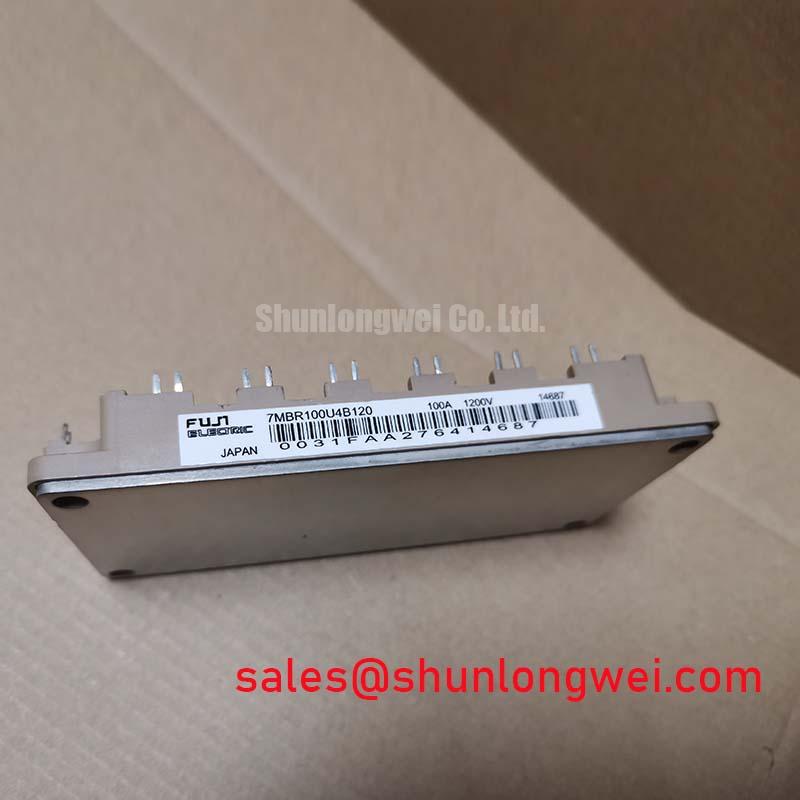
Check the terminal drawing before connecting test leads: Manufacturer: Fuji Electric | Part Number: 7MBR100U4B120-50 | Collector-Emitter Voltage (Vces): 1200.0 V | Continuous Collector Current (Ic): 100.0 A | Package: Fuji Power Module | Configuration / Topology: IGBT Power Stage | Product Category: PIM | Series: 5th Gen U-Series. Consult the manufacturer datasheet for rating conditions, terminal assignments, and assembly limits.
I check the driver auxiliary supply and its inhibit signal with the DC link disconnected before allowing a switching command to reach the 7MBR100U4B120-50. As a Design Consideration, the driver should establish a controlled gate-off state before the power stage becomes energized. Where the equipment uses negative turn-off bias, its magnitude belongs to the qualified gate-drive design, not to a value inferred from the module designation. Observe the actual gate-to-emitter voltage during auxiliary supply rise, shutdown, and interrupted startup.
Before that powered check, establish a cold measurement baseline. Identify collector, emitter, and gate connections from the terminal drawing rather than terminal position alone. With the module isolated from parallel circuit paths, use the meter’s diode function to compare corresponding power paths with consistent lead polarity. Record the instrument, connection orientation, and module temperature alongside the readings. An unexpected result warrants checking the schematic and external connections; a single forward-voltage reading does not establish switching health or remaining service life.
Bench Tip: Use ESD controls, keep gates in their specified off-state termination, and compare cold readings only after disconnecting and verifying discharge of the DC link.
During auxiliary power testing, monitor the supply at the driver rather than only at the control board connector. Cable impedance, local decoupling, and startup loading can make those waveforms different. A supply dip that crosses the driver’s undervoltage lockout threshold should produce a defined inhibited output. Check that the system does not release its switching enable while that output remains indeterminate. These are Design Considerations for the external driver; undervoltage protection is not established merely by the module’s PIM category.
The 7-in-1 converter-inverter-brake topology also makes schematic tracing important. Distinguish the converter path, inverter switching paths, and brake connection before assigning test points or interpreting a diode measurement. Related power-stage documentation, including the 7MBR10NF-120, can support a broader converter or auxiliary-stage comparison, but its circuit role and ratings must be evaluated independently. It is not an instruction to add another module ahead of this PIM.
On a controlled switching bench, measure gate voltage locally between the relevant gate and emitter terminals using appropriately rated instrumentation. A controller-referenced trace can conceal emitter movement caused by shared return impedance. As an Engineering Recommendation, separate the gate return from load-current routing wherever the equipment layout permits, and assess the resulting waveform under the intended operating conditions. Distinguish a genuine gate excursion from probe-loop pickup before changing driver components.
Protection checks should follow the external driver’s actual fault sequence. Desaturation detection requires coordination among its sensing network, blanking interval, fault latch, and turn-off behavior. A collector-emitter voltage increase during conduction is an input to that protection assessment, not proof of one particular failure. Evaluate soft shutdown against the device’s documented short-circuit operating limits and the measured collector-voltage overshoot. A startup test should not be turned into an uncontrolled short-circuit test to demonstrate protection operation.
Keep DC-link precharge and driver startup as separate checks. Precharge controls capacitor charging stress, while driver sequencing controls the state of the switches; one does not replace the other. Record which interlocks prevent energization, which inhibit switching, and how the equipment responds when auxiliary power disappears first. This gives the repair engineer a reproducible sequence for investigating startup trips without attributing every event to the replacement module.
Benchtop Waveform Tuning: Mitigating Stress via Optocoupler vs Digital Coreless Transformer Drivers on 7MBR100U4B120-50
Compare the installed isolation driver’s input command with its output gate waveform while observing the emitter reference movement. The useful distinction between an optocoupler and a coreless-transformer driver is not the technology name alone. As a Design Consideration, assess propagation behavior, common-mode transient immunity, output sink capability, supply supervision, and fault reporting together. These are properties of the selected driver and board implementation, not additional specifications of the Fuji Electric module.
For an unwanted pulse, first establish whether it exists at the driver input, driver output, or only in the measurement arrangement. A pulse already present at the input points toward the command path or its reference. An output disturbance coincident with a switching-node transition requires examination of common-mode coupling, driver supply movement, and gate-loop impedance. Compare repeatable captures with the equipment’s known-good behavior instead of treating every narrow excursion as confirmed false turn-on.
Miller coupling provides a physical reason to examine the off-state gate waveform closely. Collector-voltage movement couples charge through the device’s collector-gate capacitance, while the external driver and return path determine how effectively that charge is removed. An active Miller clamp, where included in the driver design, should be assessed at the module connection rather than assumed effective from its presence on a schematic. Do not assign this model an unverified Miller charge, capacitance, or clamp requirement.
Negative bias and clamping solve related but different gate-control problems. Negative bias changes the off-state operating point; a clamp provides a local discharge path under its specified activation conditions. Neither substitutes for checking gate-emitter limits during both normal switching and faults. As an Engineering Recommendation, investigate oscillation with the complete loop in view: driver output impedance, gate resistance, wiring geometry, emitter reference, and probe placement. Component changes should follow the observed mechanism rather than a generic gate-resistor prescription.
Isolation assessment requires separate attention to the driver barrier, board spacing, connectors, and module-to-heatsink interface. Do not transfer a driver’s isolation test voltage or reinforced-insulation classification to the complete assembly. Likewise, the module’s 1200.0 V collector-emitter rating is not an insulation withstand rating. Compare the applicable insulation test procedure with the actual terminals being tested, and disconnect circuitry that the procedure excludes. Test voltage, duration, and acceptance criteria belong to the approved equipment procedure.
For replacement evaluation, the 7MBP100RA120 is a separate comparison candidate, not an established drop-in substitute. Check its internal circuit, terminal functions, control interface, protection responsibilities, outline, and cooling arrangement against the original assembly. A similar current or voltage class cannot establish interchangeability when the host board expects a different drive architecture. The decision should rest on documented interface compatibility and a controlled validation plan.
Mechanical assembly can also affect repeatability during waveform comparison. Complete the prescribed heatsink mounting process before comparing loaded switching captures, and keep the thermal interface condition consistent between tests. Disturbed grease coverage or uneven seating can change operating temperature and obscure whether a waveform difference arose from a driver change. Mounting torque and interface thickness must follow the applicable assembly instructions rather than a general value associated with a visually similar housing.
Engineers evaluating this module for an industrial inverter welder or medium-frequency induction-heating power supply should compare the required switching duty, circuit configuration, protection interface, and cooling system with the equipment design. These are compatibility examples, not statements that every such power supply accepts this PIM. In particular, the 100.0 A collector-current rating needs its specified thermal and operating conditions before it can inform an equipment-level load assessment.
7MBR100U4B120-50 Operational Boundaries: Evaluating Baseplate Thermal Grease Layer Control Limits
Inspect the heatsink contact surface and the module mounting face before applying fresh thermal interface material. Remove residual compound using an approved cleaning method, then check for debris, raised damage, and interference around mounting features. As a Design Consideration, the interface should fill surface irregularities without becoming an unnecessarily thick thermal barrier. Select the application method and material quantity from the assembly process rather than imposing a universal grease thickness on the Fuji Power Module package.
Contact quality depends on both surfaces, not just the appearance of the applied grease. Surface flatness, permissible baseplate curvature, compound behavior, and clamp loading interact during assembly. Do not attempt to compensate for an unacceptable mechanical mismatch by adding more compound or increasing fastener torque. Use the specified inspection method to determine whether the heatsink and mounting arrangement remain suitable. A visually continuous grease coating alone does not demonstrate low interface thermal resistance.
Bring mounting screws into engagement without forcing the module into position. Where the manufacturer’s assembly procedure specifies staged cross-pattern tightening, follow that sequence with the correct calibrated tool and final torque. Avoid treating terminal fasteners and mounting fasteners as interchangeable torque applications. Inspect nearby busbars and brackets for preload that could distort seating as they are connected. The module should not become the mechanical alignment tool for an incorrectly positioned power assembly.
For a removed assembly, an uneven compound witness pattern can guide further inspection, but it does not uniquely identify the source of overheating. Compare the pattern with surface condition, mounting sequence, airflow or coolant performance, and the equipment’s temperature records. Repeat observations under comparable load conditions before assigning significance to a temperature difference. Changes in switching losses or cooling performance can produce similar symptoms even when the thermal interface appears satisfactory.
Junction-temperature assessment should connect measured case or heatsink conditions with the manufacturer’s thermal data and the actual power-loss profile. A heatsink sensor does not directly measure semiconductor junction temperature during a switching transient. The Junction temperature Application Guide provides broader thermal-management context; its seventh-generation discussion does not establish specifications for this 5th Gen U-Series part. Keep device-specific thermal limits separate from general technology explanations.
Check the upstream protection arrangement before returning the assembled stage to service. As a Design Consideration, semiconductor fuse coordination requires the fuse’s let-through energy and interruption behavior to be assessed with the circuit’s prospective fault current and documented device withstand limits. An I²t figure by itself does not establish that an IGBT will survive a fault. Driver shutdown and fuse interruption serve different time-dependent roles, and neither supports an unqualified claim of damage-free fault clearing.
Finish the assembly check by inspecting terminal alignment, restoring protective covers, and repeating the approved static and insulation checks before controlled energization. Record the module identification, cold-test connections, mounting procedure, interface material, and observed protection response in the equipment service record. If heating remains uneven, return to the measured contact condition and cooling path before changing gate-drive settings to compensate for a mechanical problem.