


Content last revised on September 27, 2026
Assembly Integrity and Transient Thermal Response for 1MBI400NP-120-01
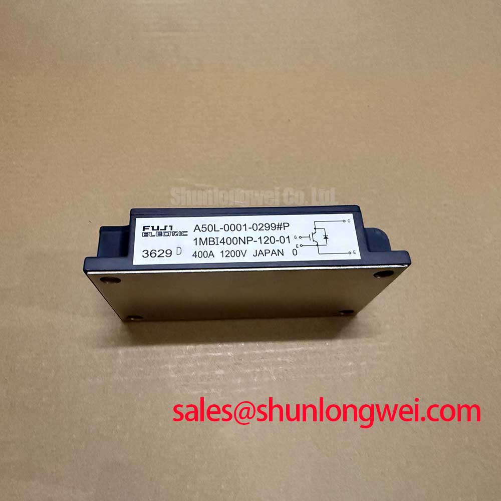
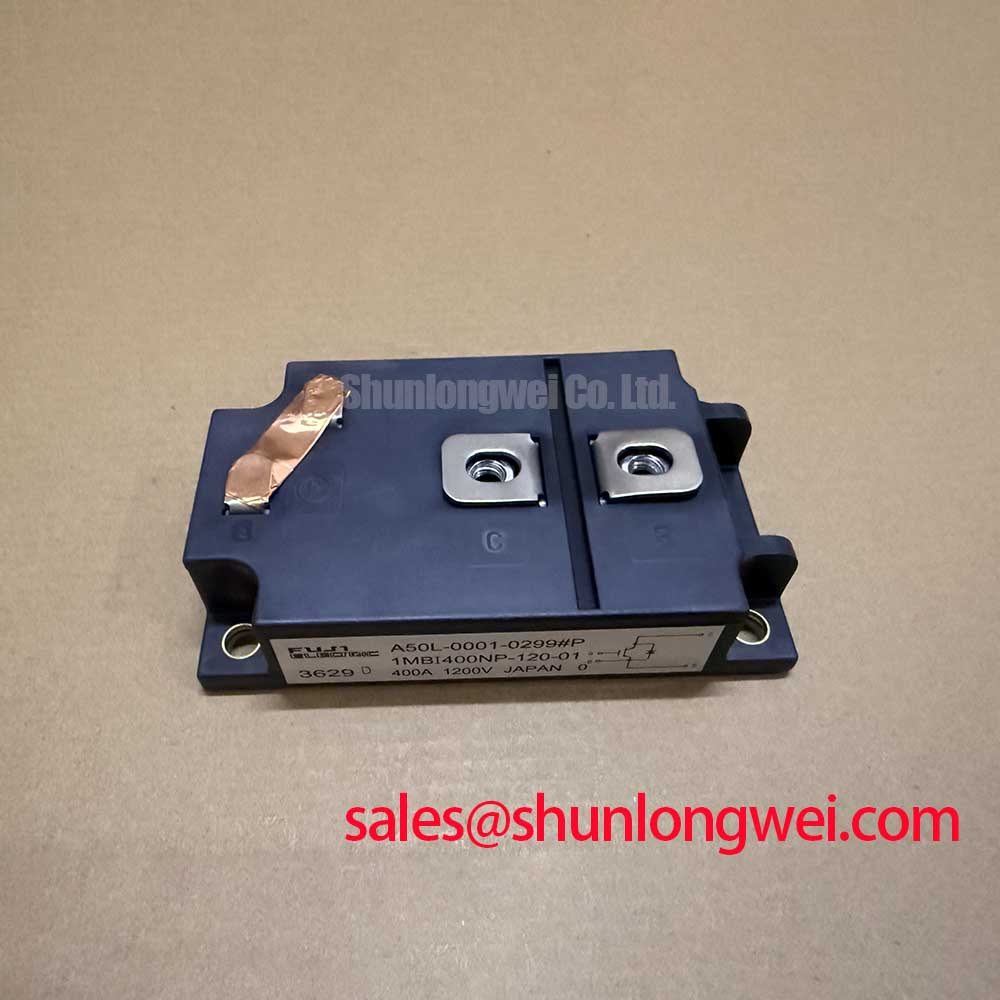
With the converter isolated and its DC link confirmed discharged, compare the cold terminal measurements of the 1MBI400NP-120-01 with the equipment schematic before connecting a gate driver. Identify the collector, emitter and gate from the applicable Fuji Electric documentation rather than assuming that another module with similar ratings shares its terminal layout. A multimeter diode-mode reading can help establish a repeatable incoming-inspection baseline, but the result depends on probe polarity and circuit connections; compare it with a documented, known-good unit instead of treating an unverified voltage reading as a pass criterion.
The 1MBI400NP-120-01 is a Fuji Electric IGBT module. Its stated continuous collector-current rating is 400 A at a case temperature of 80 °C, while its pulsed collector-current rating is 800 A. These are distinct operating conditions: a pulse rating does not establish how long an installed converter can sustain an overload.
| Parameter | Official Specification |
|---|---|
| Collector-emitter voltage | 1200 V |
| Continuous collector current | 400 A at Tc = 80 °C |
| Pulsed collector current | 800 A |
| Maximum junction temperature | 150 °C |
| Junction-to-case thermal resistance | 0.085 °C/W |
| Short-circuit withstand time | 10 µs |
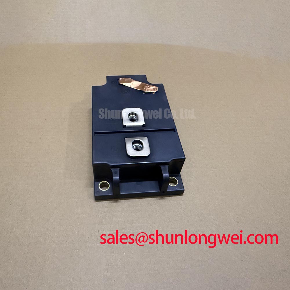
Before mounting, inspect the module’s external mounting surfaces and terminals, then compare the heatsink contact area and mounting arrangement with the original assembly. As a Design Consideration, uneven contact or disturbed thermal interface material can change the installed thermal path; the stated junction-to-case resistance does not include the entire path from case to ambient. Follow the applicable mechanical documentation for fastening and interface preparation rather than assigning a torque or interface thickness from a different package.
For a heavy current pulse, the steady-state 0.085 °C/W value alone cannot establish peak junction temperature. An Engineering Calculation would combine the measured case-temperature starting point, the pulse loss waveform and the module’s applicable transient thermal-impedance data to estimate junction-temperature rise, then compare the result with the 150 °C maximum junction-temperature specification. Transient calculations often use RC representations; Foster and Cauer thermal network models explain the distinction between transient and steady-state thermal behavior. Without a verified transient model and loss data for this module, a numerical pulse-temperature margin would be speculative. For broader context on evaluating thermal paths during repair, see The Advanced Thermal Management Revolution.
DC-Bus Headroom and Protection Coordination
The 1200 V collector-emitter rating is an Official Specification, not a suggested DC-bus operating setpoint. As a Design Consideration, the engineer should measure switching overshoot at the module terminals under representative load, temperature and fault-recovery conditions. Bus voltage, wiring inductance and turn-off behavior all contribute to the observed peak; the system design determines the required operating headroom.
Altitude and atmospheric radiation can be relevant to high-voltage semiconductor reliability, but this product data does not establish a site-specific single-event-burnout rate, FIT value or altitude derating curve. A Design Consideration for an elevated installation is to request applicable manufacturer guidance and evaluate the actual bus-voltage profile. Neither the voltage rating nor an assumed altitude threshold supports a numerical lifetime prediction for this unit.
The 10 µs short-circuit withstand time is an Official Specification that must be read alongside its applicable test conditions. It does not mean that a system fuse will clear every fault within that interval. When checking protection coordination, compare the driver’s detection and turn-off sequence, fault-current path and candidate fuse clearing behavior under the converter’s actual prospective fault conditions. Fuse I²t data and the module’s pulsed 800 A rating describe different tests; they should not be treated as interchangeable energy limits.
For a replacement assessment, 2MBI400TB-060-01 can be examined as a separate candidate, not assumed to be a direct substitute. Verify circuit configuration, voltage and current ratings, terminal assignments, mounting geometry and drive requirements against both sets of documentation before considering a change to the installed design.
Gate-Drive Loop Geometry and Switching Boundaries
Trace the installed gate-drive path from the driver output to the module gate and back through its specified emitter reference. As a Design Consideration, keeping that loop compact can reduce parasitic inductance and help limit gate ringing during switching. Check the actual terminal designation before routing a separate sensing return: the information supplied here does not establish that 1MBI400NP-120-01 has an auxiliary Kelvin emitter terminal.
On a scope capture, compare gate-to-emitter voltage at the module terminals with the driver-side waveform. A difference between the two may indicate wiring impedance or coupling through the power-current return; confirm it under controlled switching conditions before changing gate components. Gate damping is a system-tuning decision, because a change that reduces ringing can also alter switching loss and turn-off overshoot.
Collector-to-gate coupling, often discussed through Miller charge and reverse-transfer capacitance, can raise the gate voltage while the opposing switch commutates. As an Engineering Recommendation, assess the measured off-state gate waveform against the driver and module limits before deciding whether active clamping or another mitigation is warranted. No charge value, capacitance value or clamp setting is established by the supplied specifications, so none should be inferred for this model.
In a converter leg, also verify that commanded dead time and the driver’s fault response prevent overlapping conduction throughout the measured switching conditions. The module’s microsecond-scale short-circuit specification is not a prescribed dead-time setting or permission to delay protection. Establish those timings from the complete power-stage and driver documentation, then validate them at the equipment level.
Incoming Diagnostics and Driver-Isolation Checks
Record cold measurements before installation, including terminal identification, diode-mode probe orientation and readings obtained with the module disconnected from parallel circuit paths. Repeat the same method on a documented reference unit when available. An unexpected result calls for a schematic and setup check first: a diode-mode reading alone cannot determine the condition of every internal current path or establish insulation performance.
💡 Bench Tip: Keep the gate protected against electrostatic discharge during incoming checks, and compare cold readings only when probe polarity and test conditions match.
Insulation testing requires particular care because the relevant barrier, test connections and acceptance criteria depend on the module documentation and the assembled equipment. Do not infer a withstand-voltage rating for 1MBI400NP-120-01 from its 1200 V collector-emitter rating. If a repair procedure calls for an insulation test, confirm the specified terminals, method and limits before applying test voltage.
Optocoupler and transformer-based gate drivers can both be evaluated for an installed converter, but this module’s supplied specifications do not certify either driver’s isolation barrier or common-mode transient immunity. As a Design Consideration, inspect the driver’s own documentation, then capture gate behavior during representative switching. If an apparent spurious pulse occurs, check the probing method, driver supply, return path and isolation interface against a known-good channel before attributing it to the module. The driver architecture and its acceptance thresholds remain system-level decisions.

