Content last revised on September 10, 2026
7MBR25SA120B Thermal-Electrical Optimization: Cosmic Ray Robustness, Voltage Derating and Practical Tuning
Begin a powered-down inspection by checking the module’s terminal condition, package surface, mounting contact, and nameplate rating before applying any test voltage. For the Fuji Electric 7MBR25SA120B, confirm that the replacement is being evaluated as a PIM power module with an inverter IGBT section, converter diode section, braking chopper section, and integrated thermistor.
| Inverter IGBT VCES | 1200 V, maximum rating at Tj = 25°C, Official Specification |
| Converter diode VRRM | 1600 V repetitive peak reverse voltage, Official Specification |
| Brake chopper VCES / IC | 1200 V / 15 A continuous rating at Tc = 80°C, Official Specification |
| Integrated thermistor R25 | 50 kΩ typical at 25°C, Official Specification |
These ratings describe the supplied device sections and should not be treated as a complete drive-system rating. The DC-link voltage, switching frequency, motor cable arrangement, gate-drive protection, cooling path, braking duty, enclosure temperature, and control-board insulation determine the allowable operating envelope. A field replacement should therefore be checked against the original drive documentation rather than selected from voltage figures alone.
When a failed drive returns from service, first record the original DC-link voltage, fault history, cooling condition, and installation altitude before replacing the module. The 1200 V inverter IGBT rating is an Official Specification at the stated test condition, but it does not establish a universal DC-bus setting for every installation. Designers should verify switching overshoot and steady-state voltage against the actual bus waveform using a properly rated differential probe.
High-altitude operation can change the insulation environment because air density decreases with elevation. Terrestrial neutron exposure and other radiation-related reliability mechanisms may also be considered in high-voltage switching equipment, but a specific SEB probability, FIT value, or altitude derating curve cannot be assigned to this module without a qualified manufacturer source and test method. Treat cosmic-ray and neutron-related failure analysis as a system reliability study, not as a field calculation based only on the printed voltage rating.
For practical evaluation, inspect the power loop for excessive stray inductance, unbalanced conductor lengths, loose bus joints, and contamination around high-potential terminals. During a controlled switching test, compare the measured peak collector-emitter voltage with the DC-link waveform and the applicable device limits. If the overshoot is excessive, the design team should review commutation-loop geometry, gate resistance, snubber behavior, busbar spacing, and switching speed. The correct values are system-determined and require measurement under the intended load and temperature range.
Clearance and creepage must be reviewed across the complete assembly, including the module terminals, copper bars, PCB supports, fasteners, insulation films, dust paths, and enclosure surfaces. A clean laboratory board may provide a different insulation condition from a production cabinet exposed to conductive dust or moisture. The appropriate spacing is determined by the working voltage, transient environment, pollution condition, material group, altitude, and applicable product standard. Do not copy a spacing value from an unrelated inverter platform.
A MOV network can support transient control when selected for the real DC-link and fault environment, but it should not be used as a substitute for low-inductance layout or validated IGBT switching control. Engineers should verify MOV continuous voltage, surge-energy capability, clamping behavior, thermal recovery, and coordination with fuses or other protective components. The module’s own voltage rating remains the reference device parameter; the external absorption network is a design consideration requiring bench validation.
For the converter path, the 1600 V VRRM diode rating applies to repetitive peak reverse voltage under the specified device conditions. Rectifier commutation, supply impedance, regenerative energy, and line transients can produce stresses that are not visible on a simple low-voltage resistance check. A cold resistance measurement can identify an obvious short or open condition, but it cannot prove dynamic reverse-recovery performance or insulation integrity.
Preventing Spurious Faults: Desaturation Detection Guidelines for 7MBR25SA120B
Desaturation protection belongs to the gate-driver and control-board implementation; the supplied hardware table does not provide a guaranteed desaturation response time or short-circuit safe-operating-area value for this particular module. Do not label a protection interval such as a sub-10-microsecond response as an Official Specification unless it is confirmed in the applicable Fuji Electric documentation.
During troubleshooting, inspect the driver supply, gate-emitter reference, isolation barrier, desaturation diode path, blanking network, and fault-reset logic as one signal chain. A nuisance trip may involve noise coupling, an incorrect reference path, an unsuitable detection threshold, delayed fault propagation, or an actual overcurrent event. Verify the signal sequence with an oscilloscope against a known-good channel rather than assigning a single cause from the fault code.
A two-stage soft turn-off strategy is a Design Consideration for reducing the rate of current interruption during a detected fault and limiting inductive voltage rise. Its timing, gate-current profile, clamp behavior, and final shutdown level must be established by the system designer from measured collector-emitter voltage, current, and driver capability. The module data supplied here does not authorize a universal gate voltage, resistor value, or soft-turn-off interval.
Dead-time must prevent simultaneous conduction in complementary devices while avoiding unnecessary distortion of the commanded motor voltage. The correct buffer depends on driver propagation mismatch, temperature, gate charge variation, layout inductance, and controller timing resolution. Designers should verify both channels at the module terminals, because a clean logic signal at the controller does not confirm that the isolated gate signals arrive with equal timing.
Common-mode transient immunity is especially important when an optocoupler or digital isolator is placed near a fast-switching power stage. Keep the isolation return paths intentional, separate high-current commutation paths from sensitive detection traces, and control the capacitive coupling area across the barrier. The selected isolator’s CMTI specification must be checked against the measured switching transient; it should not be inferred from the presence of an isolation component.
If a drive reports an intermittent gate or desaturation fault, remove power and compare the affected phase with the remaining phases for terminal contamination, cracked solder joints, damaged driver components, and abnormal cold impedance. After repair, use a current-limited test arrangement and confirm gate-to-emitter waveform quality before reconnecting the motor. The test should include startup, low-load switching, controlled acceleration, deceleration, and fault-response observation.
Preventing Spurious Faults: High-Frequency Common-Mode Bearing Current Guidelines for 7MBR25SA120B
Long motor leads can behave as transmission-line structures at the switching edge. Cable impedance, motor winding capacitance, shield termination, cabinet bonding, and inverter output impedance can combine to produce terminal ringing and common-mode current. A reflected waveform may exceed the local DC-link level substantially in some installations, but the magnitude cannot be stated for this module without cable, motor, layout, and switching measurements.
For a high-dynamics CNC axis or robotics servo evaluation, capture the phase-to-phase and phase-to-ground waveforms at the motor terminals as well as at the module output. Compare the two locations to identify cable reflection, connector discontinuity, or grounding-related behavior. A measurement taken only at the inverter may miss the stress experienced by the motor insulation and bearings.
Output filters, common-mode chokes, dv/dt filters, and sinusoidal filters should be considered according to the motor insulation class, cable length, switching frequency, allowable voltage rise time, leakage-current limit, and servo response requirements. Filter selection is not a fixed accessory specification of the 7MBR25SA120B. The system integrator should verify filter impedance, resonance behavior, thermal loading, and interaction with the drive control loop.
Layout work begins with the physical separation of the high-current switching loop and low-level feedback wiring. Avoid routing encoder, thermistor, current-sense, and fault lines alongside the motor phase conductors for long parallel distances. Terminate cable shields and cabinet bonding according to the equipment EMC architecture, while recognizing that the power module itself does not independently carry a complete CISPR or EN 55011 certification for the finished machine.
The integrated thermistor provides a useful temperature-sensing element for the thermal protection strategy. Its specified value is 50 kΩ typical at 25°C. The control board must use the correct resistance-temperature interpretation from the applicable documentation and should validate the sensing circuit against wiring resistance, connector condition, ADC tolerance, and the intended trip logic. A resistance reading outside the expected cold-state behavior may warrant checking the sensor circuit and connector before condemning the power stage.
External MOVs and capacitive suppression components should be coordinated with the motor filter and cabinet grounding scheme. An MOV that clamps one transient may increase leakage or alter the common-mode current path. Engineers should confirm temperature rise, repetitive pulse duty, and post-event condition during representative switching tests. Protection components must be physically located so that their own connection inductance does not defeat the intended transient path.
The broader topology affects the stress seen by the module. For engineers comparing conventional rectifier-inverter arrangements with bidirectional AC conversion, the Matrix Converter Topology provides a useful reference for power-flow and commutation concepts, but it is not a direct topology statement for this Fuji Electric PIM.
Benchtop Waveform Tuning: Mitigating Stress via Dynamic Braking Chopper Operation on 7MBR25SA120B
Before testing the braking function, confirm the DC-link discharge procedure, braking resistor connection, chopper command path, and thermal sensor behavior. The braking section of this module is specified at 1200 V VCES and 15 A IC continuous at Tc = 80°C. These are Official Specifications for the stated conditions, not a complete braking-energy guarantee for a particular motor or duty cycle.
Braking-resistor selection must begin with the mechanical system’s stored energy, expected deceleration profile, DC-link operating range, resistor pulse capability, average thermal load, and fault response. The resistor must be evaluated for both peak pulse stress and repeated braking cycles. The motor inertia, reflected load, regenerative controller behavior, and stopping requirement determine the energy that the braking path must absorb.
During bench tuning, monitor DC-link voltage, chopper collector-emitter voltage, braking current, resistor temperature, and fault timing together. A rising DC-link voltage during deceleration may result from insufficient braking energy capacity, a command-timing issue, wiring impedance, or a measurement artifact. Verify the waveform with an appropriately rated probe and compare the event with the controller’s braking command before changing the power-stage parameters.
The internal chopper rating does not remove the need for an external resistor with suitable insulation, pulse endurance, airflow, and fault containment. The resistor enclosure should prevent contact with heat-sensitive wiring and should maintain the required clearance from grounded metalwork. The complete braking assembly also needs a defined failure response, such as controlled shutdown or independent overvoltage protection, established by the machine safety design.
When the module is installed, the thermal interface should be clean and uniform, and the mounting hardware should follow the original mechanical documentation. Uneven pressure can affect thermal contact and introduce mechanical stress into the package. ⚠️ Field Alert: Disconnect the DC link and verify the discharge state before touching power terminals or removing gate-drive connectors.
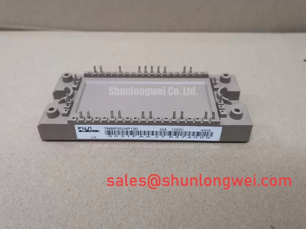
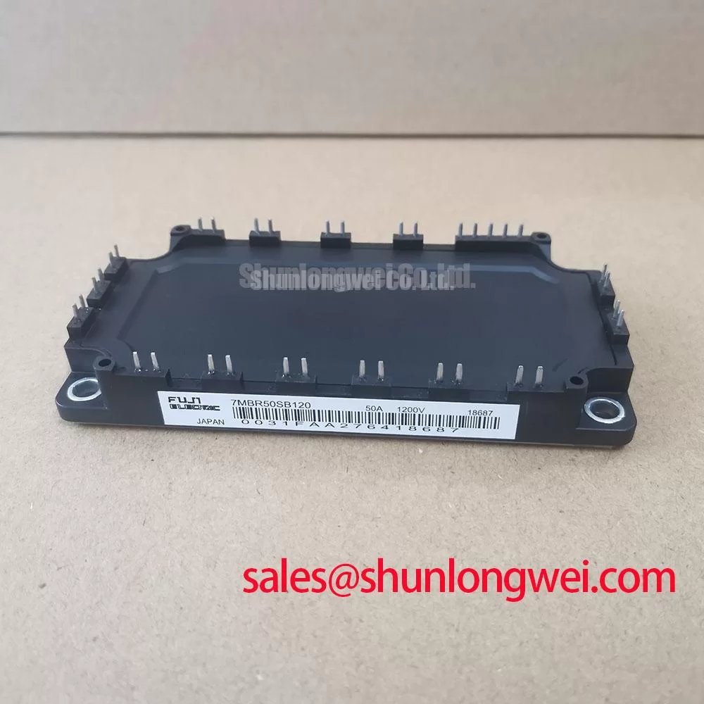
For procurement and repair planning, the neutral evaluation of a related Fuji Electric module such as 7MBR35UA120 should include pin assignment, circuit configuration, mechanical dimensions, thermal ratings, and controller compatibility rather than model-number similarity alone. In the wider power path, engineers may also review 7MBR50SB120-01 as a separate rectifier or complementary-stage reference, subject to the original equipment documentation.
For installation teams that need a broader design reference, IGBT Design & Integration covers gate-drive coordination, thermal management, and circuit-topology considerations. Final acceptance testing should be performed in the target drive with its actual bus voltage, motor, cable, cooling system, braking resistor, protective network, and control firmware.