Content last revised on September 10, 2026
Fault-Clearing Dynamics: Type-I/II Desaturation Detection and Inductive Clamping
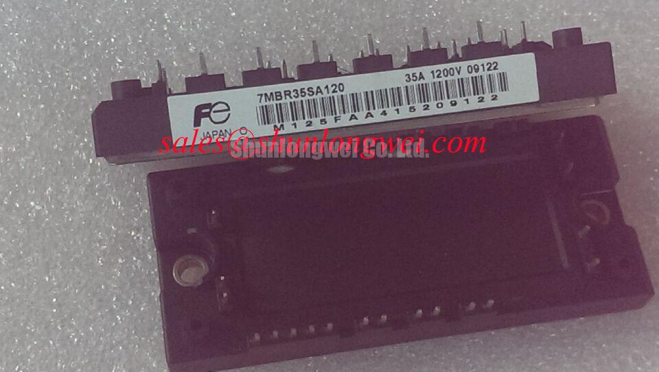
Operating precision stepper and brushless DC (BLDC) servo actuators introduces severe dynamic transitions, where sudden mechanical stalling or winding short-circuits can trigger rapid overcurrent events. Within the Fuji Electric 7MBR35UA120 power integrated module (PIM), the inverter output stage is rated at a collector-emitter voltage of VCES = 1200V (Official Datasheet Specification). Under catastrophic short-circuit conditions, the device must be safely commutated within its short-circuit safe operating area (SCSOA) boundary, which mandates a maximum short-circuit duration of 10 µs (Official Datasheet Specification). Field engineers typically categorize these occurrences into Type-I faults, where the IGBT turns on into an existing dead short across motor phases, and Type-II faults, where an insulation breakdown happens while the IGBT is already actively conducting.
When implementing desaturation (DESAT) detection via external high-voltage sensing diodes, calibrating the blanking filter and trip reference requires balancing false-tripping noise immunity against structural die survival. The trip voltage threshold is typically targeted between 6.5V and 8.0V (Design Consideration for 1200V trench IGBT architectures). When a fault is identified, executing an abrupt hard gate turn-off generates an excessive rate of current decay (-di/dt) across the internal parasitic loop inductance (Lσ). This inductive reaction generates a dangerous turn-off voltage spike that can exceed the 1200V breakdown margin. Implementing a two-stage soft turn-off (STO) network decreases the gate voltage gradually over 2 to 5 µs, limiting the overvoltage excursion. For dynamic braking control during rapid servo deceleration, the dedicated brake chopper stage features a rated collector current of IC = 20A (Official Datasheet Specification). Auxiliary chopper supplies running alongside the main drive stage should maintain stable transient recovery, drawing from established principles of Buck Converter Step-Down Voltage Regulation. Comprehensive fault diagnosis and curve tracing methods can be cross-referenced within the Field Engineer’s Handbook.
Optimizing Gate Drive Loop Geometry to Prevent Cross-Conduction Oscillation
High-bandwidth servo positioners demand rapid gate charge transfer to minimize switching losses during micro-stepping and continuous vector orientation. In the 7MBR35UA120 module, parasitic layout inductances can induce spurious gate-emitter oscillations if the control loop is coupled into the high-current emitter output. When the main load current rapidly changes, voltage drops across the emitter bond wires can inject ground bounce back into the drive circuitry. Separating the auxiliary Kelvin emitter connection from the power emitter return isolates the sensitive gate drive reference from heavy phase currents, suppressing unwanted common-mode feedback.
💡 Pro Tip: Route the auxiliary Kelvin emitter and gate conductor as an intimate twisted pair or parallel trace strip directly to the driver output stage. Keeping total gate drive loop parasitic inductance below 15 nH prevents resonant ring frequencies from overlapping with the IGBT turn-on transconductance bandwidth.
Thermal mounting accuracy directly impacts long-term die stability under cyclic servo accelerations. Module heat sinking requires a flat, milled surface with an overall flatness tolerance under 50 µm over a 100 mm span (Design Consideration). Applying a uniform thermal interface material (TIM) layer targeting a 50 to 80 µm bondline thickness prevents micro-void formation and dry spots. Fastening the casing requires a progressive diagonal cross-pattern torque sequence: snug all mounting screws to a preliminary 0.5 N·m, followed by a final tightening to 2.5 to 3.5 N·m (General Industry Design Consideration for standard M4/M5 chassis mountings). For higher-capacity servo drives requiring substantial output currents beyond the integrated 35A stage, engineers can evaluate high-capacity discrete alternatives such as the 6MBI450U-120A-02 six-pack module for modular multi-axis architectures.
Negative Gate Bias vs Active Miller Clamping in Fast-Switching Half-Bridges
The half-bridge inverter phase legs inside the 7MBR35UA120 experience sharp collector-emitter voltage transients (high dv/dt) when the opposing complementary IGBT switches on. This steep voltage step pumps displacement current through the collector-gate feedback capacitance (Cres / Miller capacitance), calculated as the product of Cres and the instantaneous dv/dt. If this displacement current passes through the internal and external gate turn-off resistance, it builds a parasitic voltage drop across the gate-to-emitter terminals. Should this voltage exceed the IGBT threshold voltage (VGE(th)), parasitic cross-conduction (shoot-through) occurs, leading to excessive power dissipation and driver thermal stress.
Two primary architectural approaches mitigate this condition. The first relies on an asymmetric bipolar power supply providing a negative gate bias between -5V and -15V (with -8V representing a Typical Starting Point for bench tuning). The negative potential establishes a safety headroom against positive displacement spikes. The alternative approach employs an unipolar 0V/+15V supply coupled with an Active Miller Clamp. In this topology, an external sensing circuit monitors the gate terminal during turn-off; once the voltage drops below approximately 2.0V, an internal low-impedance transistor shorts the gate directly to the emitter reference, shunting the Miller current away from the main pull-down path.
The integrated front-end three-phase converter bridge features a repetitive peak reverse voltage rating of VRRM = 1600V (Official Datasheet Specification). This rating accommodates 400V/480V AC utility line fluctuations under the operating guidelines of the IEC 60146 Semiconductor Converters Standard. Module temperature surveillance is managed by an integrated negative temperature coefficient thermistor exhibiting an NTC resistance of 5 kΩ at 25°C (Official Datasheet Specification). For dual-inverter designs or isolated multi-level configurations, the complementary 2MBI450UE-120 provides a dual-pack alternative for high-current sub-assemblies.
High-Altitude Cosmic Ray Induced SEB Failure & FIT Rate Mitigation
Precision motion stages deployed in elevated terrain or sub-alpine manufacturing sites face increased exposure to atmospheric terrestrial neutron flux. Energetic atmospheric neutrons can collide with the silicon lattice within the high-field drift region of the 7MBR35UA120, triggering localized electron-hole avalanche multiplication. If the electric field across the space-charge layer is sufficiently intense, this avalanche event can run away into catastrophic Single Event Burnout (SEB), permanently puncturing the chip without any prior thermal warning.
The Failure-in-Time (FIT) rate driven by terrestrial cosmic rays exhibits strong exponential dependence on the continuous DC-bus operating voltage and operating junction temperature. Although the module is officially rated at VCES = 1200V (Official Datasheet Specification), running continuous bus voltages near the maximum rating at altitudes above 2000 meters accelerates SEB risk. Applying voltage derating preserves long-term system reliability (Design Consideration based on terrestrial neutron radiation guidelines):
- Maintain continuous steady-state DC bus levels between 540V and 680V during continuous run conditions.
- Limit deceleration dynamic regeneration peaks to 800V through the integrated 20A brake chopper circuit.
- Allow a minimum 35% margin between peak repetitive bus excursions and the 1200V VCES ceiling.
When conducting field maintenance, verify the creepage distance (minimum 10.5 mm) and clearance distance (minimum 6.0 mm) across the external terminal pattern, ensuring no conductive contamination compromises tracking resistance in high-humidity or sub-atmospheric environments.