Content last revised on September 10, 2026
Optimizing Gate Drive Loop Geometry to Prevent Cross-Conduction Oscillation
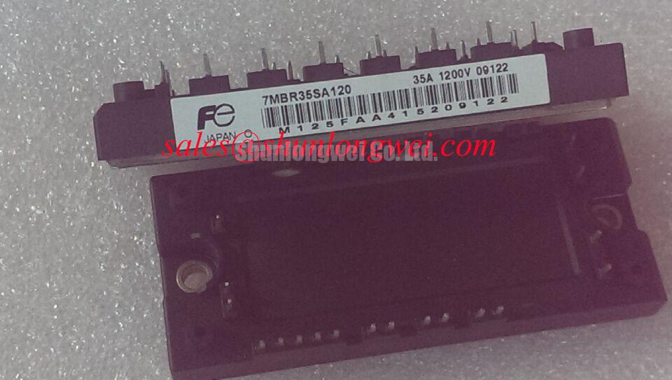
The 7MBR35SA120 integrates a 7-in-1 Power Integrated Module (PIM) architecture containing a three-phase input rectifier, a dedicated dynamic brake chopper, and a three-phase inverter output stage. Operating on 400V to 480V AC distribution grids, the inverter section requires precise gate drive management to switch its 1200V, 35A IGBT switches cleanly under heavy inductive loading. In high-bandwidth BLDC and precision stepper servo actuators, high switching speeds generate rapid collector-emitter voltage transitions (dv/dt) and current transients (di/dt). When transient currents flow across shared circuit paths, parasitic emitter inductances generate unintended voltage drops that couple directly back into the gate-emitter terminal path.
To prevent parasitic gate-source ringing and the catastrophic risk of shoot-through cross-conduction, PCB layouts must isolate the auxiliary Kelvin emitter return pin from the primary high-current power emitter trace. In the 7MBR35SA120, routing the auxiliary emitter pin exclusively to the isolated gate driver reference plane ensures that the high load current flowing through the main busbars does not induce dynamic offsets across the gate drive threshold. Implementing asymmetric gate drive conditioning—using dedicated paths for forward turn-on and reverse turn-off—allows engineers to tune turn-on dv/dt independently from turn-off di/dt. A typical starting point for bench tuning employs a gate turn-on resistor between 15 Ω and 33 Ω, paired with a lower impedance turn-off resistor (3.3 Ω to 10 Ω) or an active Miller clamp circuit.
When the complementary high-side switch fires, the rapid rise in collector-emitter voltage pushes displacement current through the internal collector-gate Miller capacitance (Cres) of the low-side switch. Without a sufficiently low-impedance turn-off path, this displacement current charges the gate-emitter capacitance above the threshold voltage (typically 5.5V to 6.5V), causing spurious conduction. Integrating an active Miller clamp transistor or providing a negative gate turn-off rail (-5V to -8V) effectively shunts this transient displacement current directly to the auxiliary emitter. For systems requiring discrete driver stages or evaluation of bare die characteristics, comparing layout geometries with Fuji Electric High-Speed Discrete IGBTs highlights how compact package pinouts minimize internal stray lead inductance.
💡 Pro Tip: Maintain tight differential routing on the gate-emitter traces from the optical or galvanic gate driver output directly to the module pins. Keep the loop area under 1.5 cm² and place bidirectional transient voltage suppression (TVS) diodes (rated for 16V to 18V clamping) directly across the gate-emitter terminals within 10 mm of the module housing. This suppresses gate overvoltage transients caused by parasitic board-level inductances during hard short-circuit fault clearing.
| Electrical Parameter | Official Specification | Engineering Relevance & Application Safety Margin |
|---|---|---|
| Collector-Emitter Voltage (VCES) | 1200V | Provides safe operating margin above typical 560V–750V DC-link levels under inductive spike transients. |
| Inverter Collector Current (IC) | 35A (@ TC = 80°C) | Supports continuous servo motor output up to approximately 11 kW to 15 kW industrial mechanical loads. |
| Saturation Voltage VCE(sat) | Typ. 2.2V (@ 35A, 25°C) | Low conduction drop directly minimizes thermal dissipation at elevated switching frequencies. |
| Thermal Resistance Rth(j-c) | 0.52°C/W (Inverter IGBT) | Enables high power density and reliable junction cooling under cyclic mechanical acceleration loads. |
| Package Integration | 7-in-1 Compact PIM | Integrates 3-phase rectifier, dynamic brake chopper, 3-phase inverter, and NTC thermistor into one unit. |
Long Motor Lead Reflected Wave Voltage & Motor Terminal Insulation Protection
In industrial automation environments, servo actuators are frequently positioned tens of meters away from the central power distribution enclosure. When the 7MBR35SA120 switches DC bus voltages exceeding 650V with transition times (tr / tf) between 50 ns and 150 ns, the high dv/dt edge travels along the motor cable as a high-frequency wave. Because the characteristic surge impedance of the motor cable (typically 50 Ω to 100 Ω) is substantially lower than the high-frequency input impedance of the motor stator windings (often exceeding 1000 Ω), a transmission line boundary mismatch occurs, causing wave reflection.
These reflected waves superimpose upon the incoming pulse front, creating terminal voltage peaks that can reach up to twice the nominal DC-link voltage (1100V to 1400V peak). Over extended operation, these repetitive overvoltage transients degrade the dielectric strength of inter-turn stator winding insulation, leading to partial discharge phenomena and premature motor failure. To mitigate these effects, design considerations include adding three-phase dv/dt output reactors, line chokes, or tuned RC snubber networks directly at the inverter output terminals. Implementing an output choke with an inductance between 0.5% and 2% impedance limits the dv/dt wavefront to less than 500 V/µs, shielding both the cable dielectric and the motor bearings from capacitive high-frequency leakage currents.
Proper module mounting directly governs physical reliability under demanding thermal cycling conditions. To maintain low junction-to-heatsink thermal impedance, heatsink flatness across the module contact area must be kept under 50 µm with a surface roughness of Rz ≤ 6.3 µm. Thermal interface material (TIM) must be applied uniformly at a controlled thickness between 50 µm and 80 µm. Excessive thermal grease acts as a thermal insulator, while inadequate application creates microscopic air voids that elevate junction temperatures.
When mounting the module baseplate, follow a symmetrical two-step cross-pattern torque sequence using M5 fixing screws. Apply an initial seating torque of 1.0 N·m across all mounting points before finalizing the clamping torque to 2.5–3.5 N·m (General Industry Design Consideration for standard M5 hardware). Adhering to this mechanical installation sequence prevents ceramic Direct Copper Bonded (DCB) substrate cracking and ensures long-term operational integrity, as outlined in the testing protocols documented within the Field Engineer’s Handbook.
Regenerative DC-Bus Voltage Surge Dissipation during Rapid Machine Deceleration
Precision motion actuators executing rapid dynamic braking transfer mechanical rotational kinetic energy back through the motor windings into the inverter stage. The integrated fast-recovery freewheeling diodes within the 7MBR35SA120 rectify this energy, routing the regenerative current directly into the main DC bus electrolytic capacitor bank. If this kinetic energy exceeds the absorption capacity of the bus capacitors, the DC-link voltage rises rapidly toward the 1200V breakdown limit of the power semiconductors.
The integrated dynamic brake chopper IGBT in the 7MBR35SA120 provides an onboard switching path to divert this regenerative energy into an external power ballast resistor. Sizing this braking resistor requires calculating the peak decelerating power and the maximum permissible pulsed collector current of the brake switch. The minimum safe resistance value is calculated to prevent peak collector currents from exceeding the rated 35A brake IGBT threshold: with an overvoltage trip setpoint of 750V DC, a ballast resistor of at least 22 Ω ensures the switch remains safely within its Forward Biased Safe Operating Area (FBSOA).
The front-end stage of the module incorporates a three-phase diode bridge rectifier capable of handling raw AC mains rectification. In complex industrial installations utilizing active power factor correction or controlled phase-angle charging, engineers often evaluate complementary switching architectures derived from Thyristor and Silicon-Controlled Rectifier (SCR) Dynamics for inrush current containment. For modular machine designs requiring distinct auxiliary power stages or secondary axis control on separated rails, related dual-switch topologies such as the 2MBI150-060 offer complementary circuit arrangements for 600V class subsystems.
Protection of the internal DC bus against short-circuit conditions requires selecting high-speed semiconductor fuses with an I²t melting integral strictly lower than the module's maximum diode surge ratings. Fast-acting semiconductor fuses placed in series with the AC line inputs limit fault energy during a catastrophic arm short, preventing case rupture and protecting surrounding system components.
Thermal Feedback & V_CE(sat) Positive Temperature Coefficient Equalization
The 7MBR35SA120 utilizes advanced IGBT silicon technology characterized by a positive temperature coefficient of the collector-emitter saturation voltage (VCE(sat)) at rated current. While low-current conduction displays a slightly negative temperature coefficient, current levels approaching the nominal 35A rating exhibit a distinct positive slope. This positive coefficient serves as an intrinsic self-balancing mechanism: if localized junction heating occurs on a particular die, the saturation voltage increases, naturally redirecting current away from hot spots and preventing localized thermal runaway.
Under intermittent high-torque acceleration cycles typical of servo positioning, power semiconductor junctions experience sharp thermal spikes. Calculating the transient peak junction temperature requires analyzing the transient thermal impedance (Zth(j-c)) network. With an inverter IGBT thermal resistance rated at Rth(j-c) ≈ 0.52°C/W (Official Datasheet Specification), short pulse durations (e.g., 10 ms to 100 ms) leverage the thermal capacity of the internal copper baseplate and DCB substrate, keeping peak junction temperatures well below the maximum rated Tj(max) of 150°C even during peak torque delivery.
The module includes an integrated Negative Temperature Coefficient (NTC) thermistor positioned on the internal substrate. This thermistor provides real-time thermal monitoring of the baseplate environment, allowing host digital controllers to implement predictive thermal derating. Because the thermistor is mounted on the substrate rather than the active IGBT silicon, there is a thermal propagation delay between the IGBT junction temperature and the NTC reading during sudden stall or lock-rotor overcurrent events. Consequently, system protection software must pair slow thermal cutoff algorithms based on NTC data with instantaneous hardware-level overcurrent desaturation (VCE(desat)) detection circuits to guard against short-duration thermal overload.
When engineering designs demand higher continuous output capacity or upgraded motor frame sizes within existing mechanical envelopes, evaluating pin-compatible or higher-power platforms such as the 7MBI100U4E-120-50 provides an established path for scaling motor drive designs while maintaining 1200V structural clearance.
| Diagnostic / Assembly Phase | Target Parameter / Specification | Field Verification & Measurement Protocol |
|---|---|---|
| Heatsink Flatness & Surface | Flatness ≤ 50 µm / Rz ≤ 6.3 µm | Inspect with precision straight edge and feeler gauges across the mounting footprint prior to paste application. |
| TIM Paste Layer Thickness | 50 µm to 80 µm uniform layer | Apply using a stainless-steel screen stencil or calibrated roller to ensure void-free surface contact. |
| Mounting Screw Torque (M5) | Pre-torque: 1.0 N·m / Final: 2.5–3.5 N·m | Use a calibrated digital torque driver following a symmetrical cross-tightening sequence. |
| Gate-Emitter Threshold Check | VGE(th): 5.5V to 6.5V | Measure with a curve tracer or high-impedance multimeter to confirm gate oxide integrity across all phases. |
| Integrated NTC Resistance | Typ. R25 = 5 kΩ (nominal @ 25°C) | Verify resistance between thermistor pins before powering up to ensure accurate temperature feedback. |