Content last revised on September 10, 2026
Desaturation (V_CE(sat)) Detection & Two-Stage Soft Turn-Off Short-Circuit Protection
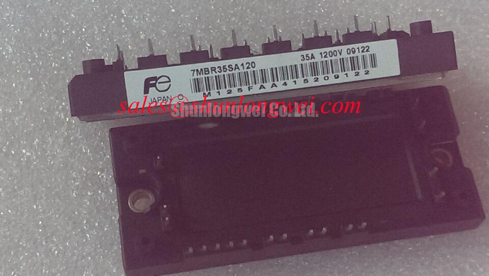
In high-reliability industrial topologies such as utility-scale 1500V solar string and central inverters, power semiconductors operate under demanding electrical stresses. In these systems, multi-level architectures (such as Neutral-Point-Clamped or Active NPC configurations) divide elevated DC-bus potentials across series-connected devices, making accurate fault detection critical. The Fuji Electric 7MBR35UB120 integrates a 3-phase inverter bridge, dynamic brake chopper, rectifier stage, and an NTC thermistor into a compact Power Integrated Module (PIM) architecture. Within the inverter section, each switch features a collector-emitter rating of VCES = 1200V (Official Datasheet Specification) with a continuous collector current rating of IC = 35A at Tc = 80°C (Official Datasheet Specification) and a typical saturation voltage of VCE(sat) = 2.15V at Tj = 25°C, IC = 35A (Official Datasheet Specification).
Short-circuit conditions in utility-scale solar conversion equipment generally fall into Type-I (fault occurrence prior to turn-on, where the IGBT transitions into a low-impedance fault) and Type-II (fault occurrence during the conduction phase, such as load short-circuits or branch flashovers). Under these fault conditions, the collector current rises rapidly, pulling the operating point out of saturation and into the active region. The Short-Circuit Safe Operating Area (SCSOA) dictates that the device must be safely isolated within 10 microseconds to prevent thermal runaway and internal bond-wire fusing.
Implementing desaturation (DESAT) detection requires setting the sensing threshold voltage above the maximum saturation envelope, where VCE(sat) = 2.60V (Maximum Official Datasheet Specification) at nominal current. Accounting for temperature-dependent forward voltage drift of the high-voltage blocking diode and the internal on-state resistance of the IGBT at elevated junction temperatures (Tj up to 150°C), a practical DESAT detection threshold typically targets 6.5V to 7.5V. The blanking capacitor must be tuned to prevent false tripping caused by turn-on voltage tailing and transient reverse recovery current spikes from the anti-parallel freewheeling diodes without exceeding the critical 10-microsecond window.
When a desaturation event is validated, hard turn-off must be strictly avoided. Rapidly interrupting fault currents exceeding four to six times rated IC produces destructive inductive voltage overshoots governed by loop stray inductance and the rate of current decay. Integrating a Two-Stage Soft Turn-Off (2SST) circuit within the gate driver mitigates this risk. Upon fault confirmation, the gate driver reduces the gate-emitter voltage from the nominal +15V to an intermediate clamping plateau (typically 7V to 9V) for a duration of 1.5 to 3.0 microseconds. This controlled reduction decreases the collector current slope prior to final isolation at -5V to -8V, containing peak transient voltages well within the 1200V absolute maximum rating. In applications requiring elevated current capability beyond the 35A threshold, engineers frequently evaluate higher-capacity configurations such as the 7MBI100U4E-120-50 to maintain equivalent safety margins under severe fault states.
Evaluating Thermal Capacitance vs Heat Sink Time Constant under Surge Bursts
Solar string and central inverters face dynamic thermal loading driven by intermittent solar irradiance, thermal cycling during grid stabilization maneuvers, and line transient disturbances. Understanding the difference between silicon-level thermal capacitance and the bulk thermal time constant of the system heat sink is necessary for maintaining junction temperatures below the 150°C maximum limit.
The 7MBR35UB120 exhibits a maximum junction-to-case thermal resistance for the inverter IGBT stage of Rth(j-c) = 0.76°C/W (Official Datasheet Specification). The silicon die possesses a very short thermal time constant (on the order of milliseconds), whereas industrial aluminum extrusion or liquid-cooled cold plates exhibit thermal time constants ranging from tens of seconds to several minutes. During severe transient bursts—such as DC-bus pre-charging surges or sudden cloud transitions in photovoltaic arrays—the junction temperature experiences steep micro-transient spikes before heat propagates through the direct bonded copper (DBC) ceramic substrate and baseplate to the heat sink.
Transient thermal management requires tracking pulse power dissipation across multi-element thermal network models (Foster or Cauer RC equivalents). For input rectification and transient protection stages, the converter section provides a repetitive peak reverse voltage of VRRM = 1600V and an average output current of IO = 35A, with a rated non-repetitive surge forward current of IFSM = 360A at Tj = 150°C, 10ms half-sine (Official Datasheet Specification). For auxiliary DC-DC pre-regulator stages operating alongside these power blocks, step-up topologies often utilize specialized control principles; design details can be explored through Boost Converter Step-Up DC-DC Conversion Principles.
To prevent dead-time shoot-through during dynamic thermal cycling, gate drive interlocking logic must enforce an adequate dead-time window (tdead). A minimum dead-time margin of 1.5 to 2.5 microseconds is recommended as a standard industry design consideration to prevent cross-conduction caused by switching delays at elevated temperatures. Continuous thermal monitoring is facilitated by the module's integrated negative temperature coefficient (NTC) thermistor, which provides a base resistance of R = 5000Ω at 25°C with a material constant of B25/50 = 3375K (Typical Official Datasheet Specification). The NTC circuit should be decoupled with a 10nF ceramic capacitor placed adjacent to the controller ADC input to filter PWM switching noise. In multi-axis or auxiliary power sub-assemblies, designers often coordinate power stages with companion compact power modules such as the 6MBI10S-120.
| Sub-Circuit Section | Key Parameter Description | Symbol | Official Datasheet Value | Unit |
|---|---|---|---|---|
| Inverter (IGBT) | Collector-Emitter Breakdown Voltage | VCES | 1200 | V |
| Inverter (IGBT) | Continuous Collector Current (Tc = 80°C) | IC | 35 | A |
| Inverter (IGBT) | Saturation Voltage (Typ / Max, Tj = 25°C) | VCE(sat) | 2.15 / 2.60 | V |
| Inverter (IGBT) | Thermal Resistance (Junction-to-Case, Max) | Rth(j-c) | 0.76 | °C/W |
| Converter (Diode) | Repetitive Peak Reverse Voltage | VRRM | 1600 | V |
| Converter (Diode) | Surge Forward Current (10ms half-sine, 150°C) | IFSM | 360 | A |
| Brake Chopper | Collector-Emitter Voltage / Current | VCES / IC | 1200 / 25 | V / A |
| Thermistor (NTC) | Resistance (25°C) / B-Constant (25/50°C) | R / B | 5000 / 3375 | Ω / K |
Baseplate Thermal Grease (TIM) Layer Control & Heatsink Mounting Torque Optimization
Efficient heat dissipation from the 7MBR35UB120 baseplate to the cooling substrate depends on the quality of the mechanical interface. The module baseplate features a slight convex pre-bow engineered by the manufacturer. This curvature ensures that when mounting screws are tightened to specification, the center of the baseplate—directly beneath the power semiconductor dies—achieves maximum mechanical pressure against the heat sink surface.
Applying thermal interface material (TIM) requires precise thickness control. Excessive thermal paste increases contact thermal resistance, while insufficient grease leaves microscopic air voids that act as thermal barriers. A uniform TIM layer thickness of 50µm to 100µm (General Industry Design Consideration) applied using a screen printing mask or automated roller is optimal. The mounting surface of the heat sink must meet strict mechanical tolerances, including a surface flatness of less than 50µm across a 100mm span and a surface roughness of Rz ≤ 10µm.
⚠️ Field Alert: Fastening mounting screws unevenly or in an incorrect sequence can permanently distort the copper baseplate, crack the internal DBC ceramic isolation layer, and cause instantaneous dielectric breakdown. Always execute a two-step fastening sequence: pre-tighten all screws diagonally to 1.0 N·m, then apply the final torque of 2.5 to 3.5 N·m (General Industry Design Consideration for standard M5 hardware). Never torque one side directly to maximum load while the opposite side remains unfastened.
Comprehensive failure analysis procedures, mechanical inspection criteria, and isolation testing standards for fielded modules are detailed in the Field Engineer’s Handbook, which provides valuable guidance for bench diagnostics and preventive maintenance schedules.
Optimizing Gate Drive Loop Geometry to Prevent Cross-Conduction Oscillation
High-voltage switching in fast-switching solar inverters generates steep voltage and current gradients. In circuits utilizing the 7MBR35UB120, minimizing parasitic stray inductances within the gate-emitter drive circuit is essential to prevent spurious turn-on and high-frequency gate oscillations. Advanced power semiconductor technologies, including wide-bandgap solutions and silicon IGBT developments, are detailed in the Fuji Electric Discrete IGBT & SiC MOSFETs technical archives.
The primary source of gate oscillation is the common emitter inductance (LE) shared between the main high-current power path and the gate-drive return path. As the collector current changes rapidly during switching, the voltage induced across LE directly opposes the applied gate voltage, slowing switching transitions and causing erratic ringing. The 7MBR35UB120 package provides auxiliary emitter terminals dedicated exclusively to the gate driver return loop. Connecting the driver ground strictly to this Kelvin auxiliary emitter pin—and maintaining complete isolation from the main DC-bus power emitter traces—eliminates mutual inductive coupling from the power loop.
💡 Pro Tip: Route the forward gate trace and the Kelvin emitter return trace as closely coupled differential pairs on adjacent PCB layers directly above an unbroken ground reference plane. Keeping total gate loop stray inductance below 15nH (Design Consideration) effectively eliminates spurious gate oscillation. In high dv/dt environments, integrate an Active Miller Clamp (AMC) circuit that shunts the gate to the negative rail through a low-impedance path whenever the gate voltage drops below 2.0V during the off-state.
High dv/dt transitions on the collector of an adjacent switch induce a displacement current through the Miller capacitance (Cres / Cies) into the off-state gate node. If this displacement current develops a voltage across the internal and external gate resistance that exceeds the IGBT gate threshold voltage (typically 5.5V to 6.5V), parasitic cross-conduction occurs, leading to arm shoot-through and catastrophic module failure. Sizing the turn-off gate resistance, utilizing a negative off-state bias voltage (such as -5V to -8V), and employing active Miller clamping provide a robust defense against cross-conduction in industrial inverter platforms.