

Content last revised on October 12, 2026
Field Diagnostics & Commissioning: Junction-to-Case Thermal Network Simulation in BSM35GD120DN2E3224 Topologies
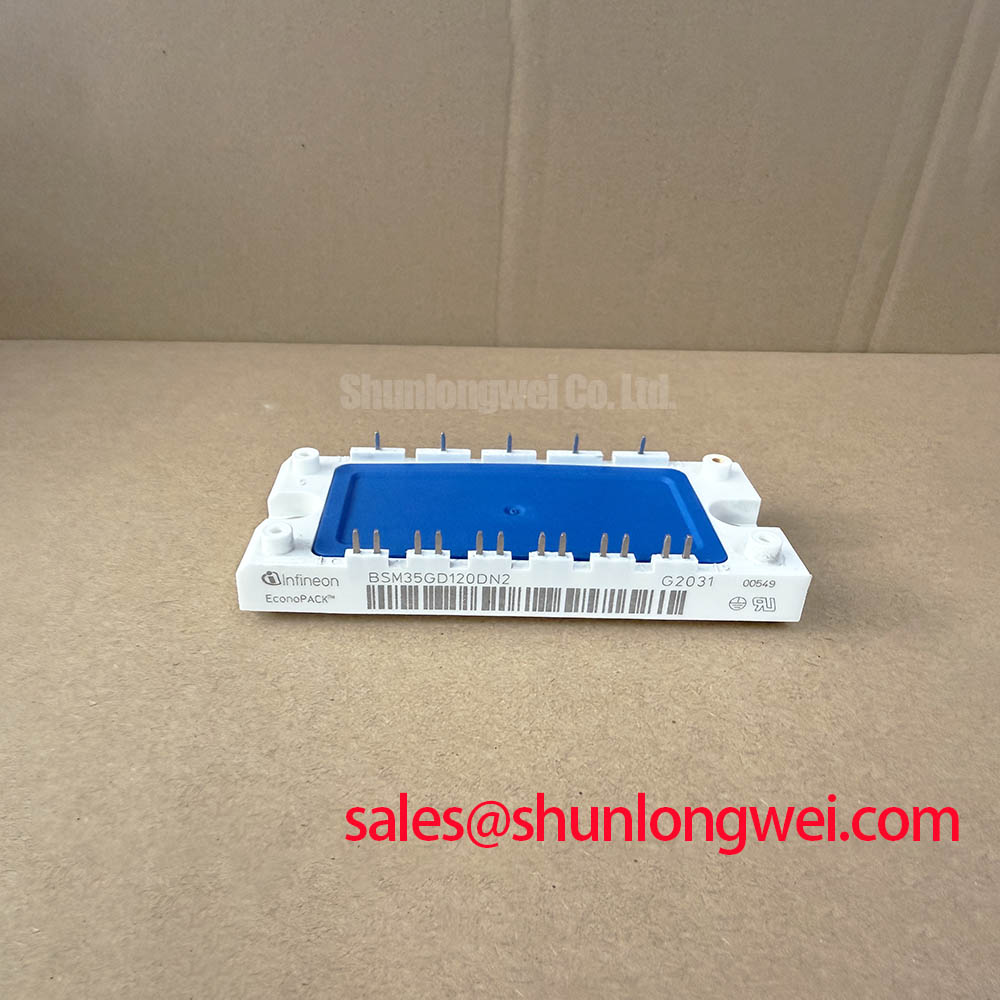
With the DC link isolated and its discharge verified, compare the terminal assignments on the installed BSM35GD120DN2E3224 with the equipment schematic before connecting a replacement module. Record the power connections, gate connections, mounting arrangement, and thermal interface condition while the original assembly remains accessible. These observations establish whether a subsequent commissioning problem belongs to the module installation, the gate-drive circuit, or the surrounding power stage.
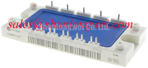
The Infineon BSM35GD120DN2E3224 is an IGBT module with a specified voltage rating of 1200 V and a rated current of 35 A under the applicable datasheet conditions. The device-specific datasheet supplies the temperature conditions, switching characteristics, terminal drawing, and mechanical limits needed to complete an electrical assessment.
For procurement and repair records, retain the complete designation shown on the BSM35GD120DN2E3224 product page. Compatibility evaluation can include a compact industrial inverter or high-speed CNC spindle drive, subject to matching the original circuit topology, drive requirements, cooling arrangement, and mechanical interfaces. A matching voltage class alone does not establish interchangeability.
Capture the overload current waveform and the corresponding case-temperature history before assigning a junction-temperature margin to a pulsed operating cycle. Design Consideration: the relevant thermal input is the semiconductor loss waveform, not simply the motor current or the cabinet air temperature. Conduction loss changes with current and junction temperature; switching loss also depends on the actual commutation conditions. Separating these contributions helps explain why similar output-current traces can produce different module temperatures.
A practical thermal model begins with the manufacturer’s transient junction-to-case thermal impedance information. A multi-RC representation can reproduce that response over the pulse durations relevant to the equipment. Keep the model type consistent: Foster and Cauer networks represent thermal behavior differently, and their internal nodes should not be interpreted interchangeably as accessible physical temperatures. The fit should reproduce the source curve across the operating interval rather than merely matching one convenient point.
For an Engineering Calculation, junction-temperature rise is obtained by convolving the time-varying semiconductor losses with the thermal impulse response, then adding the appropriate case-temperature boundary condition. This approach accounts for accumulated heat from preceding pulses. An isolated overload calculation can underestimate the peak when the next acceleration or braking event begins before the module has cooled. Use the actual repeated operating sequence when evaluating peak temperature and recovery between events.
Keep the junction-to-case model separate from the case-to-heatsink interface and the heatsink-to-ambient path. A case-temperature measurement does not directly reveal the junction temperature during a short overload. Conversely, a slow heatsink measurement can conceal a local interface problem. Position sensors consistently, document the measurement location, and compare equivalent load sequences so that changes in mounting quality are not confused with changes in the electrical operating point.
At the mounting interface, inspect contact surfaces for contamination, raised edges, and residual material that prevents even seating. Apply thermal interface material according to its application instructions and the module mounting requirements; an arbitrary coating thickness is not a substitute for controlled coverage. Follow the specified fastener sequence and torque for the actual assembly. Neither a generic bolt size nor another module’s installation practice establishes the correct tightening value for this part.
Uneven temperature behavior warrants a coordinated check of interface contact, cooling performance, phase loading, and gate-drive behavior. Compare corresponding locations under repeatable conditions rather than assigning a single cause from a thermal image. If losses increase after a drive-board repair, inspect switching transitions as well as the heatsink: slower switching or unintended gate activity can add heat without an obvious change in commanded load.
For service-life assessment, keep the discussion tied to measured thermal cycling and the equipment’s operating profile. The Wide Bandgap Revolution provides broader technical background on semiconductor technology and integration challenges, not a lifetime qualification for this module. Altitude-related insulation requirements and cosmic-ray susceptibility require their own applicable standards or manufacturer evidence; they cannot be quantified from the voltage and current ratings.
Field Diagnostics & Commissioning: Sizing Braking Resistors and Chopper Transistors in BSM35GD120DN2E3224 Topologies
Trace the regenerative-current path from the motor-side switching stage to the DC-link capacitor and braking branch before selecting a braking resistor or chopper transistor. Design Consideration: the module designation alone does not establish that a braking switch is included. The equipment schematic and terminal diagram determine which semiconductor handles braking current and whether that function belongs to a separate assembly.
Resistor assessment should start with the mechanical energy returned during deceleration, including driven-load inertia and any energy supplied by the process. The required absorption duty depends on deceleration duration, repetition, and the energy retained or transferred elsewhere in the system. Evaluate pulse-energy capability and cooling between events alongside average dissipation. A resistor with an adequate continuous power rating can still be unsuitable for the actual pulse profile.
The chopper assessment has a different emphasis: current during conduction, voltage during blocking, switching losses, and protection response. Its operating envelope must also cover the intended braking cycle and credible abnormal conditions. Set resistance, switching thresholds, and protective actions from the complete equipment design, then validate the resulting DC-link behavior. These are system decisions, not additional specifications of the BSM35GD120DN2E3224.
When checking wiring, distinguish DC-link terminals, phase outputs, and any dedicated braking connections using the relevant drawings rather than connector position. Assess creepage and clearance against working voltage, insulation requirements, pollution conditions, and installation environment. Route braking-current conductors so that their switching loop does not unnecessarily couple into gate-control wiring. Secure busbars with the specified hardware and support arrangement so mechanical loading is not transferred into module terminals.
Selection comparisons should preserve these functional distinctions. The Infineon FF300R12KE3G is a separate module reference for a broader component assessment, not an asserted replacement for the BSM35GD120DN2E3224. The following comparison identifies the information that must align before either part can be considered for an existing power stage.
| Selection item | BSM35GD120DN2E3224 | FF300R12KE3G comparison requirement |
|---|---|---|
| Manufacturer | Infineon | Infineon |
| Rated voltage | 1200 V — compare the applicable datasheet conditions | Consult Datasheet; compare rating and operating conditions |
| Rated current | 35 A — compare the specified temperature conditions | Consult Datasheet; compare temperature conditions |
| Package classification | Module — compare the specified mechanical details | Compare outline, mounting interface, and terminal arrangement |
| Circuit and drive compatibility | Use device-specific circuit and gate data | Compare topology, gate requirements, and switching behavior |
| Braking function | Establish from circuit diagram and equipment schematic | Establish independently; do not infer interchangeability |
During controlled deceleration testing, record DC-link voltage together with braking-command activity and branch current. A rising bus voltage can reflect inadequate energy absorption, inhibited switching, wiring discontinuity, or control behavior; the correlated traces distinguish these possibilities. Inspect the resistor connection and protective interlocks before attributing the symptom to the power module. Any test involving energized power terminals belongs within the equipment’s approved electrical-safety procedure.
Field Diagnostics & Commissioning: Turn-Off di/dt-Induced Peak-Voltage Clamping in BSM35GD120DN2E3224 Topologies
Measure collector-emitter voltage and gate-emitter voltage during turn-off with probes and connections suited to the switching environment. Design Consideration: parasitic inductance in the commutation path produces an additional voltage contribution as current changes. Probe-loop pickup can imitate or exaggerate that overshoot, so validate the measurement arrangement before modifying the gate drive or adding a clamp.
Reduce the physical area of the commutation loop by coordinating the module terminals, local DC-link connection, and return path. Closely coupled outgoing and return conductors can reduce stray inductance, while balanced geometry can avoid unnecessary differences between comparable current paths. Preserve the required insulation spacing and mechanical support while refining the layout. The acceptable inductance follows from measured switching behavior and voltage margin, not an arbitrary universal layout target.
Pro Tip: Keep corresponding busbar current paths geometrically balanced to reduce avoidable turn-off overshoot, then verify voltage margin through a controlled double-pulse test of the assembled power stage.
Snubber or clamp selection should follow the measured transient and an assessment of where the switching energy is transferred. Capacitor placement, connection inductance, repetitive heating, and resistor dissipation all affect the result. Increasing capacitance without checking the associated current can exchange one problem for another. Evaluate the modified waveform and component temperatures across the intended operating range, including conditions that produce the highest switching stress.
At the gate circuit, inspect the driver return path and its coupling to the power-current path. Miller coupling can disturb the gate voltage during rapid collector-voltage transitions; the measured gate waveform helps distinguish this from a commanded transition. Gate impedance, driver sink capability, and any Miller-clamp function should be assessed together. The Infineon EiceDRIVER™ galvanically isolated gate-driver IC resources provide manufacturer information for evaluating driver functions and isolation characteristics without implying that every driver is compatible with this module.
If the existing drive board uses a bootstrap supply, observe the floating supply voltage through the complete switching sequence. Recharge opportunities, high-side conduction duration, driver consumption, and leakage determine whether the supply remains adequate. Evaluate the bootstrap capacitor and diode against their actual charge-transfer and repetitive-current duties. Diode recovery and layout coupling should be considered where supply disturbances coincide with switching transitions; do not prescribe a capacitor value from module current rating alone.
For the final switching assessment, correlate voltage overshoot, gate disturbance, current commutation, and protection timing rather than reviewing each trace independently. Manufacturer material within Infineon High Power Semiconductor Solutions offers supporting device and application resources. Record the installed gate-network configuration, busbar arrangement, thermal boundary conditions, and measurement setup with the commissioning traces so that a later repair can reproduce the tested configuration.