Content last revised on October 29, 2026
6MBI450U-120A-02 Thermal-Electrical Optimization: Multi-Module Parallel Current Sharing Practical Tuning
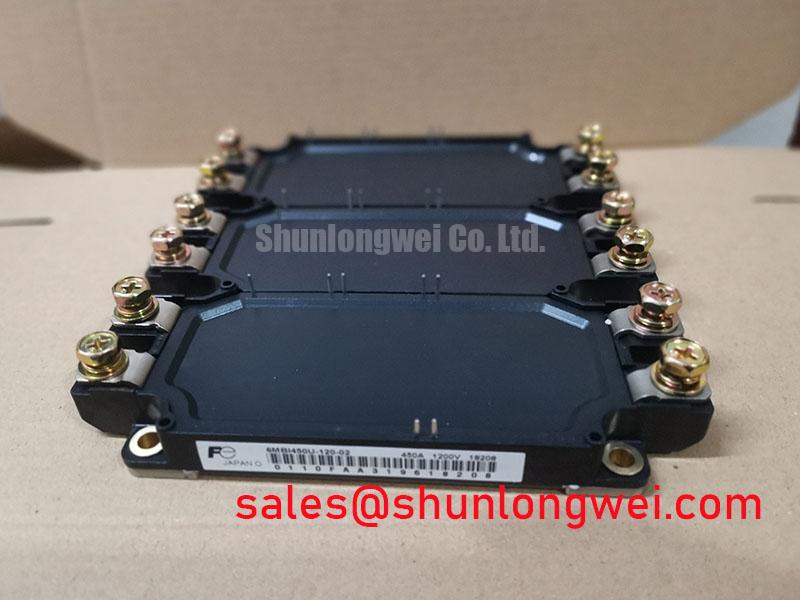
With the DC link isolated and verified discharged, disconnect the gate-driver connections before comparing cold-state terminal readings across equivalent switching positions. On a stopped converter, this helps separate a power-stage abnormality from a driver-board loading effect without treating a single meter reading as a diagnosis. The Fuji Electric 6MBI450U-120A-02 is an IGBT module rated at 1200 V collector-emitter voltage, with collector-current ratings of 450 A at a case temperature of 25°C and 300 A at 80°C; these are Official Specifications, not interchangeable operating conditions.
Record the complete suffix, terminal arrangement, driver connections, and mounting interface before removing the assembly. The Official Specifications also identify a ±20 V gate-emitter limit, 1.90 V typical collector-emitter saturation voltage at a junction temperature of 25°C under the specified test conditions, and an approximate module weight of 450 g. For repair assessment, the saturation-voltage figure is a reference operating point, while the gate-voltage figure is an absolute boundary rather than a recommended drive setting.
Compare individual branch currents at the same commanded load before changing gate resistance or disturbing the cooling assembly. As a Design Consideration, unequal current sharing can originate in unequal conduction paths, different case temperatures, gate-drive timing, or measurement error. Capture branch current and case temperature together: a current mismatch observed during a switching edge requires a different investigation from one that develops after the assembly reaches thermal equilibrium.
The supplied 1.90 V typical Vce(sat) at 25°C does not establish the temperature coefficient across the operating range. Positive temperature dependence of on-state voltage can assist static current sharing where the device characteristics exhibit that behavior, but it should not be assumed from a single typical value. For this module, evaluate the relevant output and temperature curves when approving parallel operation, and compare voltage drops under matched current, gate-drive, and temperature conditions. Do not select parallel partners solely because their room-temperature meter readings resemble each other.
For dynamic balance, an Engineering Recommendation is to keep gate and return paths electrically symmetrical and avoid routing one module’s drive return through another module’s switching-current path. Compare driver propagation timing and the actual gate-emitter waveform at each module, rather than relying only on signals measured at the controller. Unequal switching behavior can persist even when the steady-state currents appear balanced. Busbar connection geometry and cooling-contact consistency also belong in the comparison because both affect how the branches divide load.
During replacement assessment, 6MBI450U-170 is a related model to compare, not an established direct replacement for 6MBI450U-120A-02. Approval should cover terminal mapping, mounting dimensions, driver compatibility, switching behavior, diode characteristics, and thermal performance. A different voltage designation alone does not establish interchangeability. Keep the original equipment configuration as the reference, and document any driver or mechanical changes before authorizing a mixed-module assembly.
Where a branch remains hotter, inspect the contact surface and cooling path before compensating electrically. Adjusting gate drive to hide a thermal-contact problem can change switching loss without correcting the original imbalance. Record the before-and-after operating conditions so that a repeat test compares the same load, coolant state, and switching pattern.
Assembly Integrity & Layout Architecture: Suppressing High dv/dt-Induced Cross-Conduction Shoot-Through for 6MBI450U-120A-02
Inspect the off-state gate waveform while the complementary switch commutates; the objective is to suppress cross-conduction, not simply produce a clean controller output. As a Design Consideration, collector-voltage transitions can couple displacement current into the gate circuit. The resulting gate excursion depends on the driver’s sinking capability, interconnection impedance, and the switching conditions at the module.
A dedicated active Miller clamp or negative off-state gate bias can be evaluated where the driver architecture supports it. Neither is a universal repair modification. Select the implementation through the driver specification and switching measurements, keeping the complete gate-emitter waveform, including ringing, within the module’s ±20 V Official Specification. Check clamp engagement at the module connection and examine the gate return path before increasing driver strength or changing the bias supply.
Trace the power terminals and gate-emitter connections against the exact module drawing before reconnecting the driver. Similar housing shapes do not establish identical pin assignments. Inspect insulation barriers, conductor spacing, and displaced hardware in the assembled position; creepage and clearance requirements follow the equipment’s insulation coordination, working voltage, and installation conditions. For vibration-exposed assemblies, use the equipment-approved fastening and locking arrangement without allowing busbar preload to distort the module terminals.
Field Alert: Do not use terminal tightening to pull a misaligned busbar into position; align the conductors first and apply the specified fastening procedure.
For desaturation protection, distinguish normal on-state collector-emitter voltage from the abnormal voltage rise being detected. As an Engineering Recommendation, coordinate sensing blanking, fault propagation, controlled turn-off, and controller inhibition against the device’s documented short-circuit limits. Excessive blanking can delay detection, while an unnecessarily abrupt fault turn-off can increase voltage overshoot. Dead time should likewise be assessed from measured switching delays and operating extremes, not copied from an unrelated driver installation. A gate clamp does not replace correctly coordinated dead time or fault shutdown.
The broader discussion in Unlocking Efficiency in Industrial Drives provides context for switching-loss and gate-drive trade-offs, but its technology-specific characteristics are not specifications for this Fuji module. For manufacturer product-family context, consult Fuji Electric’s IGBT module portfolio, including its seventh-generation X-Series; family information should not be transferred to this part without a matching device specification.
Benchtop Waveform Tuning: Mitigating Stress via Bi-Directional DC-DC Buck-Boost Conversion on 6MBI450U-120A-02
Capture current reversal and switching-node voltage together when evaluating a bidirectional conversion stage. A useful compatibility example is a utility-scale centralized battery energy storage PCS, where engineers may assess this module for a battery-side conversion subsystem. That assessment depends on the actual circuit arrangement, voltage range, driver, cooling system, and protection coordination; the module rating alone does not establish suitability for the complete PCS.
As a Design Consideration, bidirectional DC-DC operation involves both power-flow directions, but “four-quadrant” operation should be defined from the actual voltage and current conventions. Battery and DC-link polarity do not necessarily reverse when power changes direction. During bench evaluation, identify which switches and freewheel paths carry current in each operating state, then compare commutation waveforms in charging and discharging operation. This prevents a successful test in one direction from concealing a more stressful transition in the other.
Inspect turn-on current peaks alongside the opposing device’s voltage recovery. Diode reverse recovery, commutation-loop inductance, and gate-drive behavior can all contribute to overshoot or ringing. Avoid assigning a recovery-softness factor to this module without the corresponding manufacturer characterization. An Engineering Recommendation is to compare switching energy, peak electrical stress, and observed oscillation under representative conditions before accepting a gate-drive adjustment. Slower switching can reduce some transients while increasing dissipation, so waveform appearance alone is not the acceptance criterion.
Heavy charge-discharge cycling can produce temperature excursions even when average power appears manageable. Evaluate the load sequence rather than a single steady operating point: repeated current ramps, dwell periods, and power reversals redistribute losses among switching devices and diode paths. Where the system permits it, designers can assess control changes that moderate abrupt thermal excursions, while checking response requirements and total loss. No service-life extension should be assigned without an applicable thermal-cycling model and validated operating history.
Coordinate semiconductor protection with the DC fault path as well as the gate driver. Fuse clearing behavior, prospective fault current, circuit inductance, and device withstand capability must be assessed together. A fuse’s I²t figure is not, by itself, evidence that an IGBT will survive a short circuit or that the assembly contains the resulting fault energy.
Assembly Integrity & Layout Architecture: Implementing Junction-to-Case Thermal Network Simulation for 6MBI450U-120A-02
Build the junction-to-case thermal assessment from the device loss waveform and the manufacturer’s transient thermal characterization, then anchor it to a measured case temperature. The 6MBI450U-120A-02 has an Official Specification of 1250 W total power dissipation per device and a maximum junction temperature of 150°C. The dissipation rating is not an unconditional continuous operating allowance or a substitute for the specified thermal test conditions.
As an Engineering Calculation method, a multi-RC network can translate time-varying device losses into junction-temperature rise when its parameters reproduce the applicable transient thermal-impedance curve. Use the network convention associated with the source data, and account separately for the thermal path beyond the case. A fitted network is a model of thermal response, not evidence of the module’s internal construction. Avoid deriving transient parameters from the power rating alone.
For pulsed overload assessment, include conduction loss and switching loss at the relevant current, temperature, and gate-drive conditions. Evaluate successive pulses until residual heating is represented; treating every pulse as starting from a cold case understates accumulated temperature. Compare the resulting peak junction temperature with the 150°C limit, with operating margin determined by the equipment’s thermal design and validation requirements. Case-temperature measurements should use a repeatable location and method so that test results remain comparable.
Inspect the heatsink surface, mounting flatness, interface-material coverage, and cooling operation before changing the model to explain a hot assembly. As a Design Consideration, thermal-interface defects can make a correctly parameterized junction-to-case model appear inaccurate because the case boundary condition is wrong. Follow the applicable mounting procedure and interface-material instructions rather than applying a generic torque or layer thickness.
The Official Specification also states 2500 V AC isolation withstand for one minute. This is a defined test rating, not a continuous working-voltage approval for the complete assembly. Keep insulation inspection separate from thermal acceptance, and use the equipment’s approved test procedure after service. Close the thermal assessment by comparing predicted temperature trends with measured load transients, correcting the loss inputs or case boundary where the evidence requires it.