

Content last revised on September 10, 2026
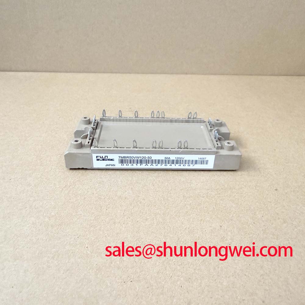
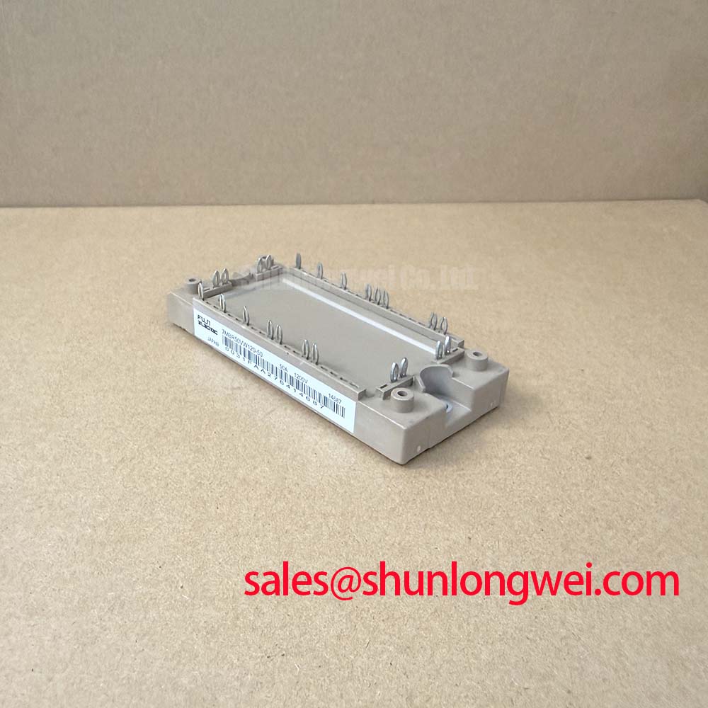
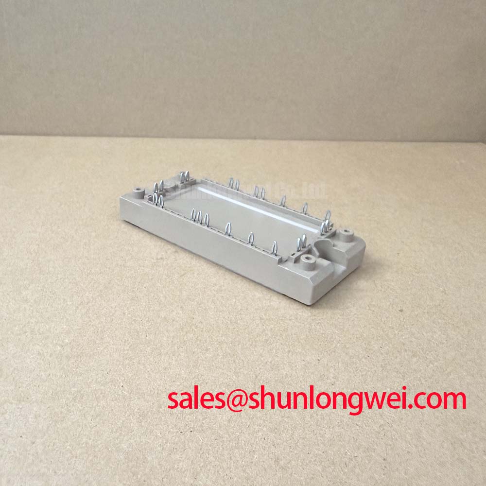
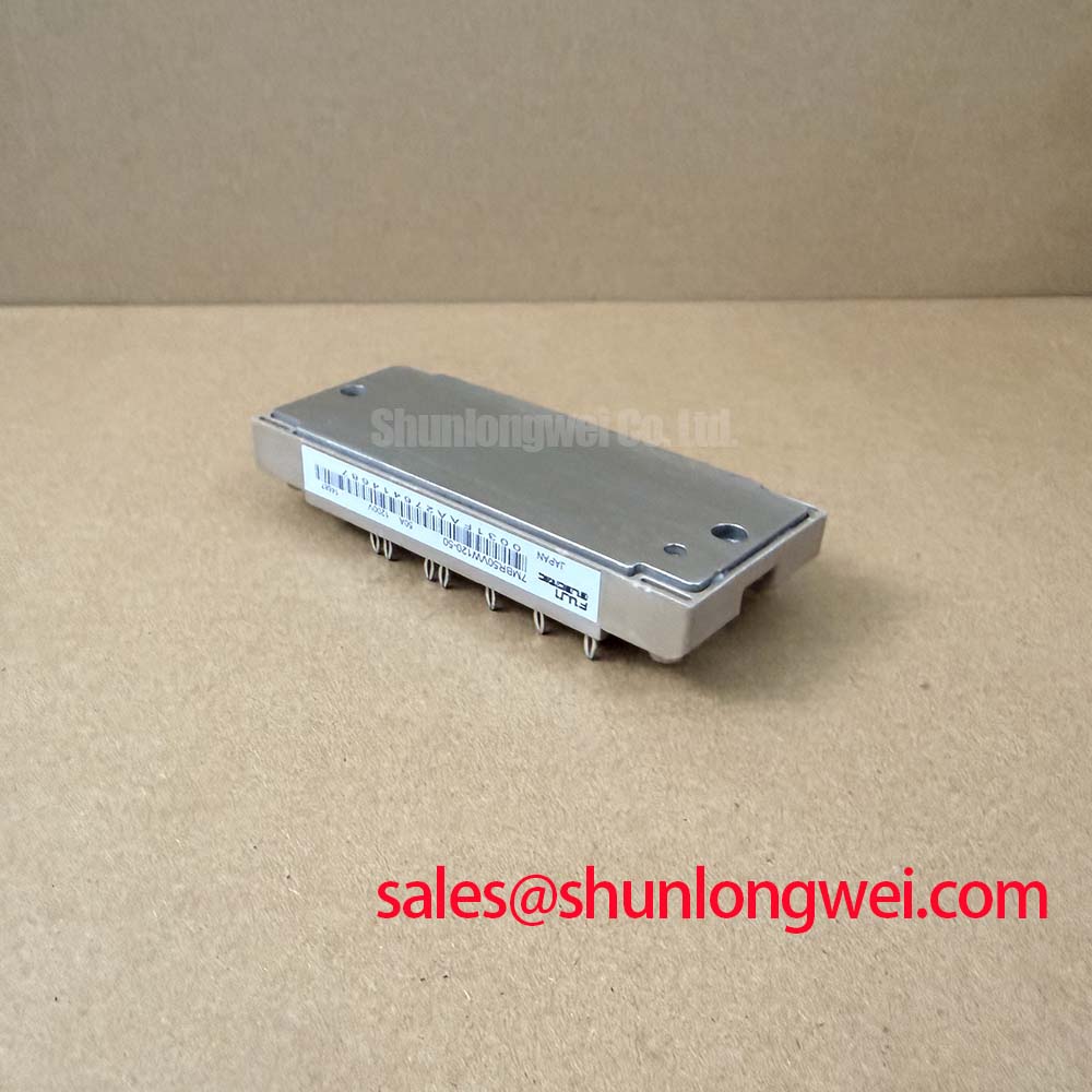
Before applying DC-bus voltage to the 7MBR50VW120-50, engineers must measure cold-state collector-to-emitter resistance across each terminal pair and confirm that the three-phase input bridge exhibits uniform forward diode conduction under multi-meter diode check. Verifying these unpowered electrical baselines prevents applying high DC rail potentials across damaged silicon, especially during board-level repair or bench prototyping. The Fuji Electric 7MBR50VW120-50 is a high-integration Power Integrated Module (PIM) housing an input rectifier bridge, an active dynamic brake chopper, a three-phase inverter output stage, and an integrated thermal sensor within a compact footprint.
Benchtop Waveform Tuning: Mitigating Stress via Transient Thermal Impedance on 7MBR50VW120-50
Thermal management under dynamic switching requires analyzing the transient thermal impedance between the semiconductor junctions and the copper baseplate. The inverter stage features rated collector-emitter voltage of VCES = 1200 V (Official Datasheet Specification), while the internal NTC thermistor provides a nominal resistance of 5000 Ω at 25°C (Official Datasheet Specification) to monitor thermal transfer in real time. Under intermittent peak-load conditions, such as sudden load steps in commercial string inverters or battery cycling in micro-grid energy storage subsystems, junction temperature fluctuations exceed steady-state thermal calculations. The thermal mass of the silicon chip absorbs energy during sub-millisecond pulses, while baseplate heat dissipation dominates during extended conduction intervals.
When modeling transient thermal behavior, engineers represent the multi-layer heat path using multi-stage RC network representations (Foster or Cauer equivalent circuits). During transient pulsed overload, peak junction temperature margin calculations must account for the instantaneous switching losses combined with steady conduction losses: junction temperature rise equals the peak dissipated power multiplied by the transient thermal impedance for the specific pulse duration. For low-duty dynamic braking cycles, the brake chopper IGBT, also rated at VCES = 1200 V (Official Datasheet Specification), undergoes rapid heating. System designers comparing power scaling options often benchmark these dissipation dynamics against lower-current modules like the 7MBR15NE120-01 to determine heatsink volume requirements and thermal derating boundaries across various power tiers.
Monitoring junction-to-case margins requires placing thermocouple probes at the baseplate periphery closest to the high-side inverter chips. Discrepancies between calculated temperatures and physical measurements often reveal uneven heatsink contact pressure or thermal grease voids beneath high-loss chip locations.
Benchtop Waveform Tuning: Mitigating Stress via SCSOA Overcurrent Protection: Implementing on 7MBR50VW120-50
The Short Circuit Safe Operating Area (SCSOA) sets rigid electrical limits during fault conditions. The module is capable of withstanding short-circuit currents up to its rated limits provided the fault is detected and extinguished within a duration under 10 microseconds. Faults are generally classified as Type I (hard switching onto an existing line short, resulting in steep current rise) or Type II (a fault occurring while the IGBT is already conducting, triggering instantaneous desaturation). When desaturation occurs, the collector-emitter voltage pulls out of saturation, generating high instantaneous power across the silicon die.
💡 Pro Tip: Keep gate loop stray inductance below 20 nH by routing the forward gate trace directly over its dedicated emitter return path on adjacent PCB layers.
To safely clear faults within the SCSOA boundary, the gate drive circuitry must incorporate desaturation detection paired with a two-stage soft turn-off (STO) sequence. Hard turn-off during an overcurrent condition generates an inductive voltage overshoot defined by peak voltage equal to the DC-link voltage plus the product of loop stray inductance and the rate of current fall. By clamping gate discharge through a high-impedance path during the first phase of shutdown, collector current fall time is extended, keeping inductive turn-off spikes comfortably below the 1200 V dielectric breakdown threshold.
High-side gate drive stability also depends directly on bootstrap power supply sizing. When selecting the bootstrap capacitor, designers must ensure that the total stored charge covers both the total gate charge requirement and the continuous driver quiescent current across the minimum switching frequency period, maintaining high-side gate voltage well above undervoltage lockout thresholds throughout continuous modulation.
7MBR50VW120-50 Thermal-Electrical Optimization: Baseplate Thermal Grease Layer Control Practical Tuning
Uniform heat transfer from the module baseplate into the heatsink requires controlled thermal interface material (TIM) deposition. Because baseplates exhibit micro-convexity engineered to flatten under mechanical torque, excessive thermal compound increases thermal impedance, while inadequate coverage causes dry contact points. Applying a uniform layer between 50 and 100 micrometers via a precision stencil or roller ensures complete wetting without dry voids across the module footprint.
| Stage / Component | Key Parameter | Symbol | Value | Engineering Significance |
|---|---|---|---|---|
| Inverter Stage (IGBT) | Collector-Emitter Voltage | VCES | 1200 V | Ensures breakdown safety margins on high DC-bus links (Official Datasheet Specification). |
| Converter Stage (Diode) | Repetitive Peak Reverse Voltage | VRRM | 1600 V | Provides high transient surge immunity from utility line disturbances (Official Datasheet Specification). |
| Brake Stage (IGBT) | Collector-Emitter Voltage | VCES | 1200 V | Accommodates dynamic braking energy clamping (Official Datasheet Specification). |
| Internal Thermistor | Resistance | R | 5000 Ω (at 25°C) | Provides real-time baseplate thermal tracking (Official Datasheet Specification). |
Mechanical mounting sequence directly dictates TIM spread and baseplate stress. Fastening requires a crosswise pre-tightening pattern: screws are threaded finger-tight, torqued to approximately 30 percent of rating, and then brought up to the target assembly specification (typically 2.5 to 3.5 N·m for standard M5 hardware under general engineering guidelines). Improper single-point torquing bends the baseplate, fracturing internal direct bonded copper (DBC) ceramic substrates. Field diagnostic techniques and mechanical inspection checklists for recurring thermal faults are thoroughly detailed in the Field Engineer’s Handbook, which serves as a practical diagnostic baseline for analyzing physical failure modes in power semiconductor modules.
7MBR50VW120-50 Circuit Protection & Reliability: Calibrating High dv/dt Cross-Conduction Shoot-Through
Rapid switching transitions in modern inverter bridges generate high collector-emitter slew rates (dv/dt), frequently exceeding 5 kV/µs. When the complementary switch turns on, displacement currents flow through the internal gate-collector Miller capacitance of the un-switched device. If the gate circuit impedance is insufficiently damped, this displacement current creates a transient voltage rise across the gate resistor, potentially exceeding the device gate threshold voltage and inducing parasitic cross-conduction shoot-through across the DC bus.
To eliminate shoot-through risks, drive architectures employ an active Miller clamp or negative gate turn-off bias (typically -5 V to -8 V). An active Miller clamp monitors gate potential during the low state; as voltage falls below approximately 2 V, a low-impedance internal MOSFET shorts the gate directly to the emitter rail, shunting displacement current away from the external turn-off resistor.
At the input stage, the three-phase converter bridge features a rated repetitive peak reverse voltage of VRRM = 1600 V (Official Datasheet Specification). This rating provides voltage margin against mains transients during AC-side surges conforming to IEC 61000-4-5 Surge Immunity Testing Standards. Utility disturbances and lightning-induced surges propagating through incoming distribution lines are clamped using front-end varistor topologies as outlined in Surge Immunity Testing (IEC 61000-4-5) for Power Mains, preserving the dielectric integrity of the converter diodes during commercial power integration.