

Content last revised on October 11, 2026
BF300R12KS4 Thermal Electrical Optimization for Gate Drive Tuning
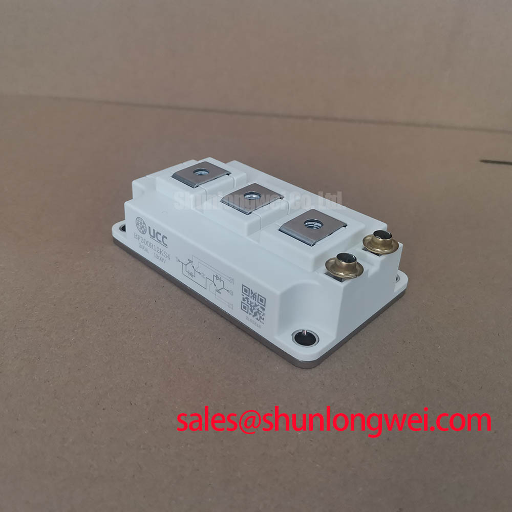
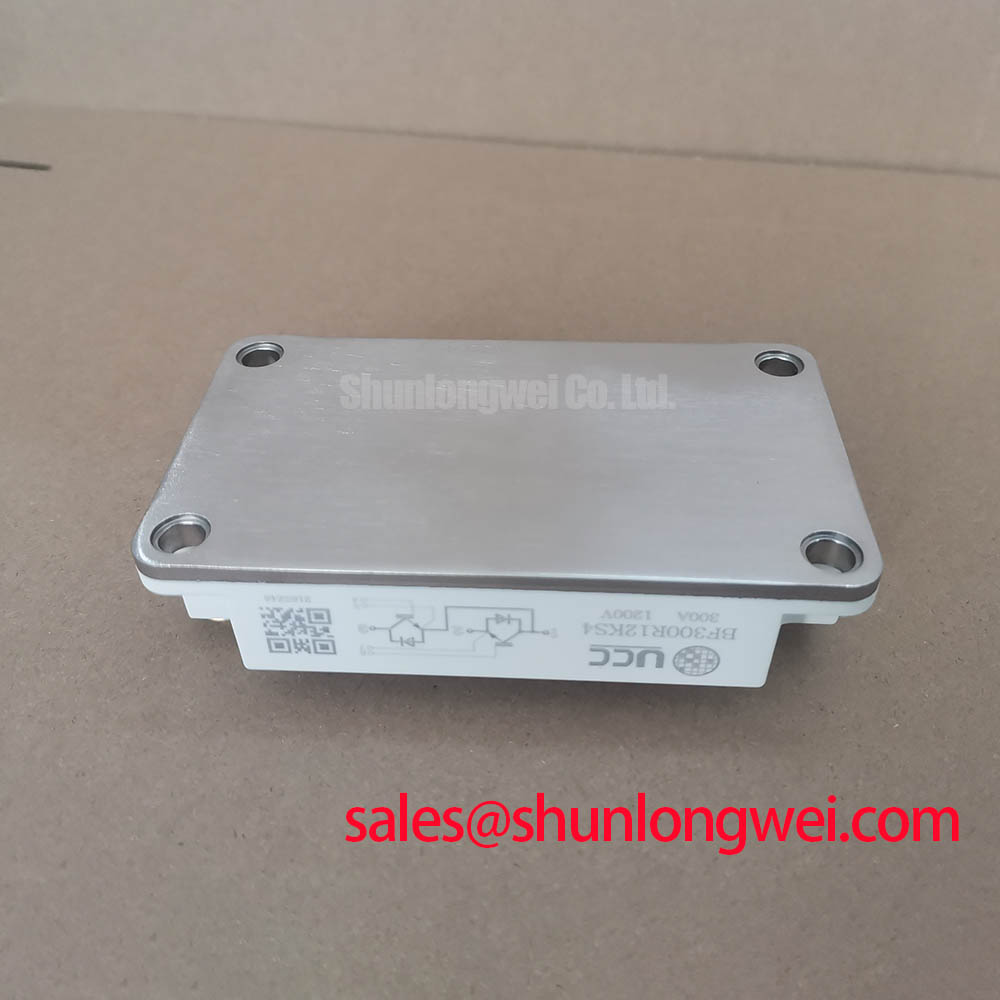
When a legacy drive board receives an Infineon BF300R12KS4, I first compare the existing gate network with the replacement module’s switching behavior before increasing the DC link voltage. The official product ratings are 1200 V and 300 A, with a PrimePACK™ 3 package designation. These values identify the electrical class of the device; they do not establish a complete operating point for a particular inverter, traction controller, or motor system.
The external turn on and turn off gate resistors should be assessed separately. A shared resistor can make a retrofit appear stable during light load testing while producing excessive switching loss at rated current. A practical engineering recommendation is to begin with the installed driver capability, gate loop geometry, and the original board’s resistor arrangement. The turn on path controls the rise of collector current and the associated di/dt, while the turn off path has a strong influence on collector voltage overshoot, ringing, and electromagnetic coupling into nearby control traces.
Do not select a resistor only from the nominal current rating. The final value depends on gate charge, driver source and sink current, isolated supply impedance, gate loop inductance, switching frequency, and the thermal limit of the complete assembly. For a retrofit, measure the gate emitter voltage directly at the module terminals rather than at the driver connector. A long probe ground lead can hide high frequency ringing and produce an unnecessarily aggressive resistor adjustment.
During commissioning, record the gate waveform and collector emitter voltage under controlled load changes. If turn on ringing increases after reducing the gate resistance, restore damping before evaluating efficiency. If turn off overshoot is present, inspect the commutation loop, laminated busbar arrangement, local DC link capacitors, and the separate turn off gate path. The relationship between switching loss and di/dt is a system result, so the engineer should verify peak voltage and junction temperature margins during switching tests rather than treating a resistor value as a fixed property of the module.
MOV coordination can provide an additional layer of transient control around the inverter input or DC link, but the MOV voltage class, energy rating, clamping behavior, and repetitive duty must match the actual surge environment. An MOV should not be used to conceal excessive stray inductance in the power loop. The preferred sequence is to reduce the source of the overshoot, confirm the remaining transient with a properly referenced differential probe, and then assess whether a surge absorber is appropriate for the equipment topology.
For an electric material handling vehicle or forklift traction controller, battery charging and regenerative braking can impose bidirectional energy flow through the DC link. Designers should evaluate the gate network during acceleration, deceleration, battery charging, and fault interruption. A stable waveform in motoring mode does not automatically represent the reverse power-flow condition.
When the original board cannot accommodate the electrical and mechanical requirements of the BF300R12KS4, the neutral comparison point may include the FZ600R12KE3. It should be evaluated by its own voltage, current, terminal, gate-drive, thermal, and mechanical requirements rather than assumed to be a direct substitute.
Assembly Integrity and Layout Architecture for the BF300R12KS4
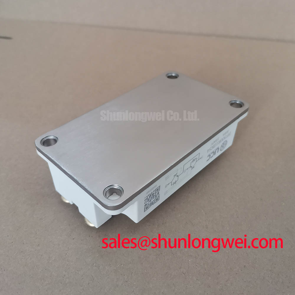
Inspect the heatsink contact surface and the module baseplate before tightening the BF300R12KS4; uneven contact can create local mechanical stress that is unrelated to the electrical quality of the gate signal. A clean, flat mounting surface supports more uniform thermal interface material distribution and reduces the chance that tightening force will be transferred unevenly into the ceramic substrate.
The commonly used 50 to 80 µm thermal interface thickness is a Design Consideration, not an official BF300R12KS4 rating. The practical target is continuous coverage without excessive material buildup. A thick layer increases thermal resistance, while insufficient compound can leave dry areas under the baseplate. Apply the selected interface material according to its own manufacturer instructions, then inspect the contact pattern when the assembly process permits it.
Use a calibrated diagonal cross pattern when tightening the mounting hardware. The purpose is to distribute pressure progressively rather than pull one corner of the baseplate down while the opposite side remains unsupported. The correct torque is determined by the module mounting hardware, heatsink construction, fastener class, and manufacturer documentation. A torque value taken from another package family should not be transferred automatically to this device.
💡 Bench Tip: Keep the module and heatsink at a known cold state, protect the terminals from ESD during handling, and compare the replacement assembly with a known good cold reference before applying the DC link.
Mechanical inspection should include baseplate convexity, heatsink flatness, burrs around mounting holes, contamination on the thermal interface surface, and any movement of the module after the first tightening pass. A visual check of the terminal alignment is also useful because mechanical strain can make a power connection appear secure while leaving uneven contact pressure at the busbar interface.
The high side gate supply requires separate attention when the driver uses bootstrap power. Bootstrap capacitor selection is an engineering calculation based on total gate charge, driver quiescent current, switching duty, leakage, temperature, bootstrap diode characteristics, and the permitted gate supply ripple. The capacitor must support the required high side on time without allowing the driver supply to approach its undervoltage lockout threshold. The correct capacitance cannot be inferred from the 300 A current rating alone because gate charge and driver behavior are separate electrical characteristics.
Keep the bootstrap charging path short and separate from noisy power commutation conductors. Place the gate driver return and emitter reference according to the driver architecture, avoiding a shared path with high current switching return. The layout should also preserve clearance around high voltage nodes and prevent the isolated control section from being exposed to unnecessary capacitive coupling.
Field Diagnostics for Long Motor Lead Reflected Wave Voltage
With long motor leads, measure the motor terminal waveform rather than relying only on the inverter bridge output. The cable and motor form a transmission path, and impedance mismatch can produce reflected-wave behavior that raises the terminal voltage well above the local bridge waveform. A frequently used worst-case design consideration is a transient approaching twice the applied DC voltage at the motor terminals, but the actual amplitude depends on cable construction, length, termination, switching edge, motor impedance, and measurement location.
For the 1200 V BF300R12KS4, the engineer should compare the measured switching peak with the insulation capability of the motor, cable, connector, and terminal system. The module voltage rating is not a substitute for checking the complete motor circuit. Use a differential voltage probe with suitable common-mode capability and place the measurement at the motor terminals when investigating reflected voltage. A probe connected only at the inverter may miss the highest stress point.
Output filters and chokes should be selected from the measured waveform, cable parameters, switching frequency, motor insulation requirements, and allowable common-mode current. A filter that is effective for one motor cable arrangement can create resonance or additional loss in another. Designers should examine the filter’s interaction with the inverter control loop and verify the thermal condition of the choke during both motoring and regenerative operation.
Busbar geometry remains important even when the main symptom appears at the motor. The parasitic commutation inductance produces an additional voltage component during rapid current change. Minimize the high current loop area, place local capacitive support close to the switching path, and keep gate control wiring away from the collector and emitter power conductors. The remaining peak margin should be confirmed during the intended switching test conditions, including low battery voltage, high battery voltage, acceleration, braking, and abrupt load changes.
When a waveform contains repeated oscillation rather than a single controlled transition, inspect the measurement setup first, then compare the gate signal, phase output, DC link, and motor terminal at the same operating point. A mismatch between these locations may indicate cable reflection, probe reference error, common-mode interference, or an interaction between the output filter and the motor. Treat the waveform as evidence for the next measurement, not as proof of one isolated component failure.
For broader topology reference, the Peak Efficiency in Solar and Energy Storage guide offers a technical foundation for examining multilevel switching paths, voltage distribution, and layout-related transient behavior. Its concepts can help structure an investigation, while the BF300R12KS4 installation still requires validation in the actual traction or industrial drive.
Preventing Spurious Power Up Shoot Through in BF300R12KS4 Topologies
Apply the auxiliary gate driver supply and confirm the driver’s undervoltage lockout state before connecting the high voltage DC link. A power stage can experience unintended conduction if the control logic becomes active while the isolated gate supply is still rising, if one channel leaves lockout earlier than its complementary channel, or if common-mode displacement moves the apparent gate emitter voltage.
A negative turn off bias is often evaluated in high power IGBT driver designs to improve immunity against Miller induced turn on. The frequently used range of approximately −5 V to −15 V is a Design Consideration for the driver and insulation system, not an official BF300R12KS4 rating supplied in the product data provided here. The final bias must be compatible with the gate oxide, driver output stage, isolated supply, protection threshold, and switching conditions documented for the selected implementation.
Power sequencing should establish a defined off state before the controller releases PWM. The gate driver should confirm its auxiliary supply, UVLO status, fault reset state, and interlock condition before the DC link contactor or precharge sequence completes. Where a bootstrap high side supply is used, confirm that the charging path is established during the intended low side state and that the high side driver does not depend on an undefined floating node during startup.
Common mode ground bounce can make a safe gate signal appear unsafe at the controller while the actual gate emitter voltage is moving differently at the module. Keep the gate loop compact, route the driver return with its signal reference, and avoid sharing the gate return with high current emitter paths unless the topology explicitly requires it. Shielding or a controlled reference plane may reduce capacitive coupling, but the effect should be checked with differential measurements at the module pins.
The protection sequence should include desaturation or overcurrent response where supported by the selected driver, a defined dead time, soft shutdown behavior, and a fault latch that prevents immediate repetitive restart. These functions belong to the driver and controller design rather than the IGBT module alone. Check the reaction path under battery charging, traction reversal, contactor bounce, emergency stop, and DC link precharge conditions.
Infineon’s OptiMOS™ Low Voltage MOSFETs information is relevant when comparing low voltage auxiliary switching stages or battery-side power paths, but it should not be treated as a substitute for the gate-drive and isolation requirements of the 1200 V, 300 A BF300R12KS4 power stage.
Before releasing the equipment for service, capture the auxiliary supply ramp, both complementary gate signals, the gate emitter voltage at the module, the DC link rise, and the first controlled switching event. Confirm that the interlock remains active during supply disturbances and that a driver fault cannot leave one bridge position conducting while its complementary position is commanded on.