
Content last revised on November 8, 2026
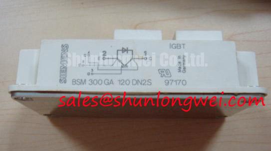
BSM300GA120DN2S Identification and Pre-Test Checks
- Isolate the DC link, verify discharge with suitable test equipment, and disconnect parallel circuit paths before comparing cold-state power-terminal measurements.
- Check the module identification against the equipment bill of materials and compare terminal positions with the original power-stage drawing.
- Inspect heatsink contact, mounting surfaces, terminal insulation, and gate-driver connections before restoring auxiliary power.
- Prepare appropriately rated differential voltage and current probes so fault signals can be correlated with gate and collector waveforms.
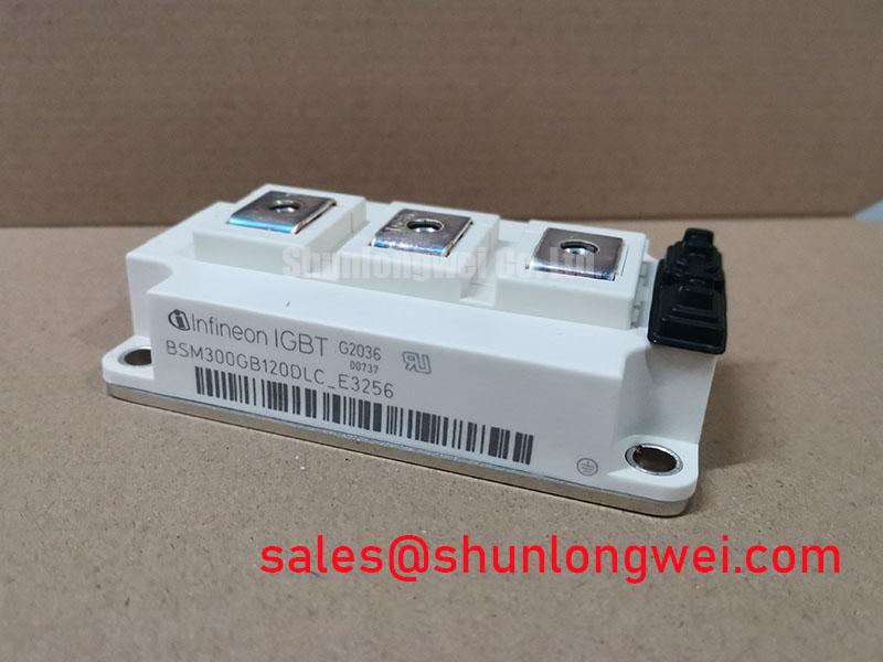
The BSM300GA120DN2S is an Infineon IGBT Module with the electrical ratings below. For repair assessment, establish the installed circuit configuration before treating a matching current or voltage rating as evidence of interchangeability.
| Parameter | Official Specification |
|---|---|
| Manufacturer | Infineon |
| Part Number | BSM300GA120DN2S |
| Product Category | IGBT Module |
| Collector-Emitter Voltage (Vces) | 1200.0 V |
| Rated Collector Current (Ic) | 300.0 A under the specified datasheet conditions; not an unconditional continuous operating current. |
| Package | Module |
| Configuration / Topology | IGBT Power Stage |
| Integration details | Consult Datasheet for terminal assignment, rating conditions, mechanical dimensions, gate limits, thermal characteristics, and short-circuit capability. |
Compatibility assessment can include industrial inverter welders and medium-frequency induction-heating supplies, subject to their actual switching topology, cooling arrangement, and protection requirements. The following integration guidance is identified as Design Consideration, rather than additional factory specifications.
Field Diagnostics & Commissioning: Fault-Clearing Dynamics and Type-I/II Desaturation in BSM300GA120DN2S Topologies
Capture the gate command, collector-emitter voltage, current, and driver fault output on the same timebase when investigating a desaturation trip. As a Design Consideration, this separates a protection response from the switching event that initiated it. A fault latch alone cannot establish whether the initiating condition was a load short, unintended simultaneous conduction, disturbed gate drive, or interference entering the detection circuit.
A Type-I short circuit generally describes turn-on into an existing short; a Type-II event develops while the device is already conducting. These conditions produce different current and voltage trajectories. Review the driver’s blanking interval, sensing network, propagation delay, and shutdown sequence against the applicable short-circuit safe operating area. Do not assign this module a generic microsecond withstand interval: protection timing must follow its documented conditions and the complete driver response.
Desaturation sensing observes collector-emitter voltage during commanded conduction, but the measured signal also contains switching transients and coupling from adjacent conductors. Route its sensing path away from noisy power connections and examine the signal at the driver input. Excessive filtering can delay a genuine trip; insufficient transient rejection can interrupt normal operation. The useful setting is established by comparing normal switching captures with controlled protection tests.
Two-stage soft turn-off is a system-level protection option that reduces gate drive before completing shutdown, moderating current fall and the associated inductive overvoltage. It must still clear the fault within the device’s permitted stress envelope. Check the fault latch and restart interlock as well as the initial turn-off waveform; repeated automatic restart into an unresolved fault is not a valid commissioning test.
At the mounting interface, preserve terminal clearances and creepage paths when installing sensing leads or protective covers. Their requirements depend on working voltage, insulation coordination, pollution conditions, and the equipment construction, rather than a spacing inferred from the module’s blocking rating.
BSM300GA120DN2S Circuit Protection & Reliability: Calibrating Output Sinusoidal Filter vs dv/dt Reactor
Measure the switching-node waveform and load-terminal waveform separately before selecting an output reactor or sinusoidal filter. As a Design Consideration for cable-fed circuits, transmission-line reflections can increase terminal stress when cable impedance, load impedance, and switching-edge duration interact. The resulting peak belongs to the complete installation; it is not a fixed multiplication factor attributable to the BSM300GA120DN2S.
A dv/dt reactor principally moderates edge behavior, while a sinusoidal filter also attenuates switching-frequency content. Choosing between them requires the actual output frequency range, modulation method, cable characteristics, load impedance, and permissible voltage drop. Check magnetic saturation, winding heating, capacitor loading, and resonance across the operating envelope. A filter that improves one measured edge can still introduce an unfavorable resonant condition elsewhere.
Keep module-side and load-side measurements distinct during troubleshooting. Collector-emitter overshoot concerns device stress, whereas a reflected load-terminal pulse concerns the cable and connected equipment. Probe placement and measurement bandwidth affect both observations. Comparing captures under equivalent conditions helps distinguish a real circuit change from a measurement artifact.
The input rectifier, DC-link capacitor network, and switching stage also interact through bus ripple and current return paths. If a separate controlled switching stage is being assessed, the BSM150GAL120DN2 provides another device record for complementary-stage evaluation, not evidence of an interchangeable rectifier function. Establish its actual circuit role before comparing electrical interfaces.
After an output-network change, revisit desaturation behavior under normal load transitions. Changed commutation currents or resonant ringing can alter the sensing waveform. Evaluate any soft-turn-off adjustment against both nuisance-trip immunity and fault-clearing requirements, rather than extending blanking simply to suppress an unexplained alarm.
Preventing Spurious Faults: Static and Dynamic Current Distribution Guidelines for BSM300GA120DN2S
Compare branch-current waveforms during switching transitions if the equipment parallels power devices. As a Design Consideration, similar average currents do not prove similar switching stress. Differences in gate-loop impedance, emitter-return inductance, power-path resistance, and local cooling can shift transient current toward one branch and produce apparently inconsistent protection events.
A positive temperature coefficient of collector-emitter saturation voltage can support static sharing only in the operating region where the device characteristics demonstrate it. Do not assume that behavior across the entire current range. Examine the relevant characteristic curves and account for junction-temperature differences before relying on thermal feedback as a balancing mechanism.
Keep the driver return separate from the high-current emitter path wherever the documented terminal arrangement permits. Where an auxiliary emitter connection is explicitly identified, use it according to that connection scheme; do not infer a Kelvin terminal from package appearance. Shared emitter inductance changes the gate-emitter voltage seen by the device during current transitions, even when the driver output appears undisturbed.
For suspected Miller-induced turn-on, observe gate-emitter voltage during the opposing switch’s transition. Evaluate return-path impedance, driver sink behavior, coupling, and any implemented clamp together. Increasing gate resistance alone can change switching loss and commutation behavior without resolving the dominant coupling path.
Pro Tip: Use symmetrical power paths and closely matched gate-return routing to limit unequal transient stress, then verify turn-off overshoot and branch sharing with appropriately controlled double-pulse measurements.
For cross-model assessment, compare the BF300R12KS4 against the required circuit configuration, terminal map, mounting interface, gate-drive behavior, and thermal limits. A related current and voltage class does not establish a drop-in replacement. Record the differences before approving changes to the busbar, driver, or cooling assembly.
Benchtop Waveform Tuning: Mitigating Overvoltage Stress in BSM300GA120DN2S Circuits
Separate a sustained DC-link rise from a brief collector-emitter overshoot before changing switching speed. As a Design Consideration, these observations point to different energy paths: regenerative energy raises bus voltage over the deceleration interval, while local commutation inductance produces a transient associated with changing current. Gate tuning cannot remove sustained energy returning to the DC link.
Where the equipment uses a braking chopper, identify its actual switching device and resistor circuit from the schematic. The BSM300GA120DN2S designation does not establish an integrated braking function. Chopper assessment should consider blocking stress, pulse current, switching loss, and thermal loading; resistor assessment should cover pulse energy, repetitive duty, cooling, and the intended discharge interval.
Observe bus voltage, chopper command, and resistor current together during a controlled test. A rising bus with absent resistor current can have several explanations, including an open circuit, inhibited control, or a protection interlock. Distinguish them through circuit measurements rather than assigning the symptom directly to the power module.
When comparing gate-drive settings, use the Switching loss Application Guide as supporting technical discussion of dynamic parameters. Relate measured switching energy to the intended operating cycle and cooling path. The Infineon IGBT Modules & Discretes Official Portfolio provides manufacturer context for device technologies; part-specific characteristics remain the basis for limits.
Repeat the relevant waveform measurements at the intended load and thermal conditions after tuning. Record collector-emitter peak voltage, gate behavior, switching energy, bus response, and protection recovery together so an improvement in one trace is not accepted at the expense of another operating constraint.