

Content last revised on November 6, 2026
BSM50GB170DN2 Inspection and Evaluation
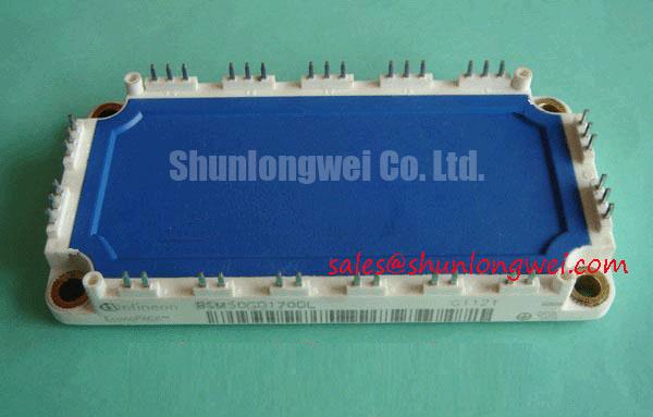
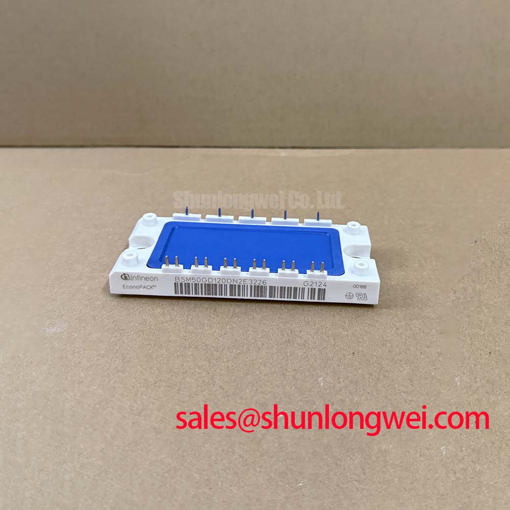
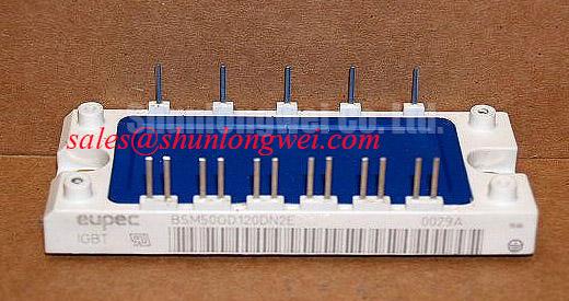
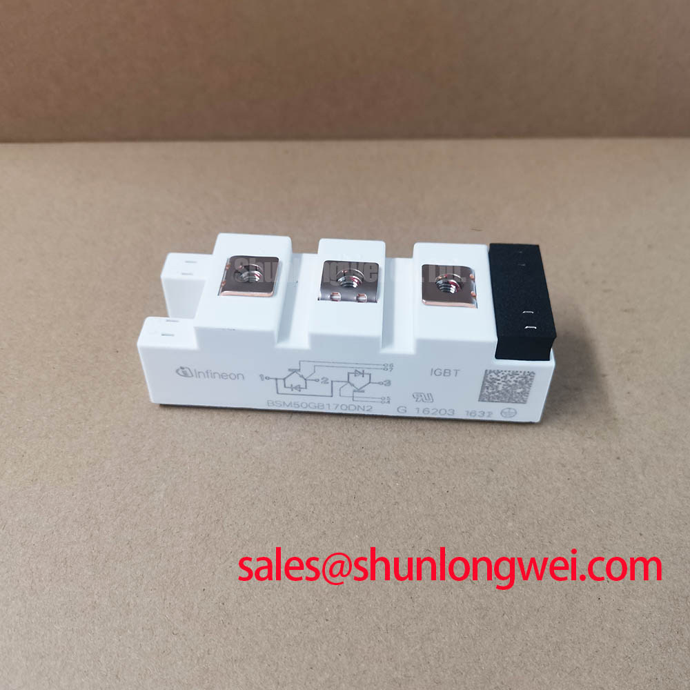
With the traction inverter isolated and its DC link confirmed discharged, inspect the module terminals and mounting surface before taking cold resistance readings across the power stage. The Infineon BSM50GB170DN2 is an IGBT Module with a specified Collector-Emitter Voltage (Vces) of 1700.0 V and Continuous Collector Current (Ic) of 50.0 A. Its listed Package is Module, and its Configuration / Topology is IGBT Power Stage.
Use those ratings as identity and evaluation data, not as a substitute for checking the inverter’s switching conditions, cooling arrangement, protection coordination, and mechanical interfaces. For a suspected in-service failure, compare measurements with the corresponding circuit and a known-good phase where available. A module rating alone does not establish a drop-in replacement; terminal layout, gate-drive behavior, thermal path, and system-level limits all affect compatibility. Infineon’s IGBT Modules & Discretes portfolio provides manufacturer-level product context.
Benchtop Waveform Tuning: Thermal Time Constants and Peak Junction Temperature on BSM50GB170DN2
For pulsed loading, assess the junction-to-case thermal response over the actual pulse pattern rather than treating the continuous current rating as a pulse-duty limit. A transient thermal model can represent heat flow through multiple time constants; the relevant inputs include the pulse duration and repetition, the initial thermal state, the case temperature, and the cooling system. Use the applicable device thermal data and the inverter’s measured operating profile to estimate peak junction temperature. Do not infer a numerical margin from the headline current rating alone.
On the bench, capture collector-emitter voltage and current during representative switching events, then correlate the electrical waveform with case temperature and cooling conditions. A waveform that changes as the unit warms can point to a thermal or drive interaction, but the trace should be interpreted alongside probe bandwidth, probe placement, and the measured gate signal. Keep the commutation path compact and minimize parasitic inductance as a design consideration; the system engineer should verify switching overshoot and temperature against the applicable device limits.
For a locomotive traction inverter evaluation, include the real operating profile rather than a single static test point: acceleration, regenerative operation, and sustained duty can impose different thermal patterns. A FP10R06KL4 can be reviewed as a separate IGBT reference, but its presence does not establish electrical or mechanical interchangeability with the BSM50GB170DN2.
BSM50GB170DN2 Thermal-Electrical Optimization: Gate Bias and Active Miller Clamping
Unintended turn-on during a fast switching edge should be investigated at the gate-emitter terminals of both the switching and non-switching devices. Common-mode transients can couple through device capacitances and layout parasitics; the resulting gate disturbance depends on the complete driver and power-stage arrangement. An active Miller clamp or a negative turn-off bias may be considered as part of a driver redesign, but neither feature nor a specific bias voltage is established here as a BSM50GB170DN2 rating.
Measure gate-emitter voltage with a suitable differential probe and a short, low-inductance measurement connection. Check the driver return path and keep gate-drive routing separate from high-current commutation paths. Where the module provides auxiliary emitter connections, confirm their pin function from the applicable package documentation before using them as a driver reference; do not assume an auxiliary terminal is present or assign a Kelvin function without confirmation.
For a bootstrap-powered high-side driver, size the supply capacitance from the driver’s charge demand, quiescent current, switching interval, and permissible supply droop. Include the bootstrap diode’s recovery behavior and the available recharge time in the assessment. These are system design considerations: validate the gate supply under the intended switching pattern and confirm that driver protection remains effective.
BSM50GB170DN2 Thermal-Electrical Optimization: Gate Driver Auxiliary Power Sequencing
Keep the DC link disabled until the gate-driver auxiliary supplies are stable and the driver’s enable and undervoltage lockout behavior has been checked. In a multi-channel traction inverter, verify that each channel reaches its intended off state during startup, shutdown, and fault recovery. A controlled sequence reduces the chance that an unsettled driver state coincides with an energized power stage.
During troubleshooting, monitor the driver supply rails, enable signals, and gate-emitter waveforms together. If a channel’s output does not follow the expected sequence, inspect the supply ramp, reset logic, interlock signals, and isolation interface before attributing the issue to the power module. Keep isolated control and power references correctly separated, and assess the isolation components’ common-mode transient immunity against the switching environment as a system-level design task.
Field alert: Keep the inverter DC link isolated during connector work, and follow the equipment manufacturer’s discharge and lockout procedure before probing or reseating driver connections.
For replacement evaluation, verify the module’s physical outline, terminal assignment, mounting arrangement, and thermal interface against the original assembly drawing. Apply the equipment’s specified fastening method and thermal-interface process; do not transfer a torque value from another module or enclosure without confirming that it applies.
BSM50GB170DN2 Circuit Protection and Reliability: Motor-Cable Transients
Long motor leads can behave as transmission lines, so reflected switching edges may increase motor-terminal stress and contribute to common-mode current. The magnitude depends on cable length and construction, motor impedance, switching edge rate, and the installation. Do not treat a particular voltage-multiplication factor as a guaranteed condition for this module or inverter.
When evaluating a drive system, compare inverter-terminal and motor-terminal waveforms using measurement equipment and probe arrangements suitable for the switching environment. If reflections or excessive edge-related stress are observed, designers can assess output filtering or a choke as system-level options, then verify their effects on switching loss, current, and protection coordination. Filter selection should follow the motor, cable, and inverter characteristics rather than the module’s voltage rating alone.
Coordinate semiconductor fuses with the inverter’s fault-current path and the module’s applicable short-circuit and thermal limits. Fuse clearing behavior and device withstand capability must be evaluated together; an I²t label by itself does not establish protection under every fault condition. For broader gate-drive design context, see the gate-driver design guide, and use the device-specific documentation when confirming terminal functions and operating limits.