

Content last revised on November 10, 2026
CM100E3U-24H Identification and Commissioning Checks
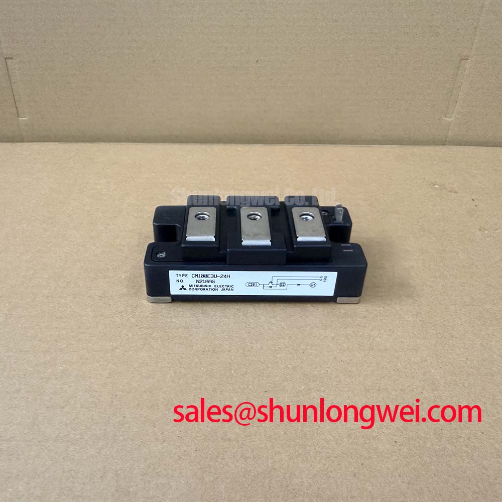
- Confirm the nameplate and part marking: CM100E3U-24H, Mitsubishi Electric.
- Check cold-state terminal behavior before connecting the DC link or gate driver.
- Inspect terminal seating, washer contact, heatsink flatness, and mechanical clearance around the module.
- Verify driver isolation, auxiliary power sequencing, and gate-return routing before applying traction-battery voltage.
The CM100E3U-24H is a Mitsubishi Electric IGBT module listed for a high-voltage power-conversion stage. Its confirmed ratings provide the starting point for evaluating inverter legs, regenerative braking converters, battery charge and discharge equipment, and low-voltage traction systems used in electric material-handling vehicles. The electrical rating does not replace system validation: the DC-link architecture, switching frequency, cooling path, gate driver, protection circuit, and load profile determine the usable operating envelope.
| Specification | Value | Engineering status |
|---|---|---|
| Manufacturer | Mitsubishi Electric | Official product identification |
| Part Number | CM100E3U-24H | Official product identification |
| Product Category | IGBT Module | Official product category |
| Collector-Emitter Voltage (Vces) | 1200.0 V | Official Specification |
| Collector Current Rating (Ic) | 100.0 A | Subject to the datasheet’s specified rating conditions; not an unconditional operating current |
| Package | Module | Official package classification |
| Device Type | IGBT Power Module | Does not specify the internal circuit topology |
| VCE(sat) | 2.9 V typical, 3.7 V maximum | IC = 100 A, VGE = 15 V, Tj = 25 °C |
| Rth(j-c), IGBT | 0.19 °C/W maximum | Junction-to-case thermal characteristic |
VCE(sat) should be treated as a conduction-loss input rather than a fixed system loss value. Actual dissipation varies with collector current, junction temperature, switching conditions, and the thermal interface to the heatsink. The published junction-to-case value applies to the IGBT portion identified in the specification and should be used with the complete thermal path when checking case temperature and cooling performance.
Field Diagnostics and Commissioning: Torque Reaction Absorption in CM100E3U-24H Topologies
Mechanical torque reaction at the main power terminals must be controlled before electrical commissioning begins. During installation, the conductor, busbar, washer stack, and terminal hardware should settle without forcing the module terminal sideways. Excessive thread engagement, uneven washer pressure, or a busbar that is pulled into alignment by the screw can transfer levering stress into internal copper joints. Vibration from traction motors and repeated heating and cooling can make this condition progressively worse.
Use a flat, supported busbar arrangement that approaches the terminal without twisting. Clearance around the module should allow the conductor to be removed and refitted without levering against the housing. The heatsink should support the module evenly, while the thermal interface should remain continuous across the intended mounting area. A tilted base, trapped debris, or uneven clamping sequence can create both thermal resistance and mechanical loading.
During a field replacement, loosen the connected busbar before judging the module terminal condition. Look for displaced washers, marks around the terminal shoulder, cracked insulation, or copper movement at the joint. These observations do not identify a single failure mechanism by themselves, so compare the affected phase with an equivalent known-good phase and review the mechanical assembly sequence. After reassembly, verify that the busbar rests naturally before final tightening and that no cable force remains at the terminal.
⚠️ Field Alert: Never insert or remove power or gate cables while the traction inverter remains energized, even when the battery contactor appears open. Isolate all energy sources, discharge the DC link according to the equipment service procedure, and verify absence of hazardous voltage before working on connections.
For electric forklifts and warehouse traction equipment, the enclosure can experience frequent acceleration, braking, and load changes. Designers should therefore inspect terminal support and heatsink attachment as part of electrical fault service, not as a separate mechanical task. The CM35MXB2-24A may be reviewed as a separate Mitsubishi Electric module option when a different voltage or current arrangement is required, but electrical, mechanical, and thermal compatibility must be established independently.
Preventing Spurious Faults: Power-Up Shoot-Through Control
Power-up sequencing should keep the gate driver in a defined off state before the high-voltage DC link reaches the IGBT power stage. Auxiliary driver supply, logic enable, UVLO status, fault reset, and gate-return reference need to be observed together rather than checked as isolated signals. A driver that appears enabled while its isolated supply is still rising can create an unwanted pulse, especially when the opposing switch has not yet reached a controlled off state.
A negative turn-off bias can be considered where the selected driver and insulation system support it. Negative gate bias is a system-level design consideration, not an official rating of the CM100E3U-24H. The gate voltage, driver output capability, isolation distance, clamp behavior, and Miller current path must be verified against the actual gate-emitter limits stated in the applicable device documentation. The objective is to prevent dv/dt-induced gate movement without exceeding the gate insulation boundary.
UVLO interlocks should inhibit high-voltage application until both relevant driver channels have stable supply status and a confirmed off command. At commissioning, monitor the driver supply and gate-emitter waveform during the contactor sequence. A brief gate excursion, asymmetry between complementary channels, or a delayed fault-reset signal warrants examination of the isolation power supply, enable logic, and return-current routing before the load is connected.
Fuse coordination belongs to the complete protection design. A high-speed semiconductor fuse should be evaluated by comparing its clearing behavior and I2t characteristic with the module’s permitted surge and fault conditions, the DC-link capacitance, and the wiring inductance. The fuse cannot be treated as a substitute for desaturation detection, gate shutdown, or a properly timed interlock. The CM400DU-24F can be referenced as a separate IGBT module when reviewing power-conversion options, while its ratings remain separate from those of this module.
In a bidirectional battery DC-DC converter, repeated charge and discharge transitions also place demand on the driver power supply and isolation barrier. Thermal cycling at the module and busbar should be reviewed alongside switching faults because a mechanically stressed terminal or drifting gate loop can appear only after the equipment reaches operating temperature.
CM100E3U-24H Operational Boundaries: DC-Link Layout and Clamping
Switching overshoot is governed by the interaction of DC-link voltage, commutation current, stray inductance, device switching speed, and the clamping network. In practical terms, the peak collector-emitter voltage rises when current changes through parasitic inductance; the relationship can be expressed during engineering analysis as the DC-link voltage plus the inductive voltage generated by the product of stray inductance and current slew rate. This is a calculation framework, not an additional rating of the CM100E3U-24H.
Place the high-frequency DC-link capacitor close to the commutation loop and keep the positive and negative conductors geometrically paired. A broad, symmetrical planar busbar generally reduces loop area compared with separated conductors. The capacitor selected for the fast loop should be evaluated for impedance, ripple current, self-heating, and physical connection inductance rather than capacitance alone. Snubber selection should follow measured ringing frequency, peak voltage, pulse energy, and thermal behavior.
During a double-pulse or equivalent switching test, use a suitable high-bandwidth voltage measurement arrangement with a short connection path. Compare the measured peak with the specified collector-emitter voltage boundary and the system’s transient protection response. If ringing changes substantially when the probe connection is moved, the measurement loop may be influencing the result. Check the DC-link capacitor connection, laminated busbar alignment, snubber location, and commutation path before changing the gate resistance.
Regenerative braking adds a second operating condition. When a forklift motor returns energy to the battery, the DC-link voltage can rise according to battery acceptance, converter control, and braking-resistor operation. The braking chopper and resistor bank should be assessed for energy absorption, thermal recovery, and fault isolation. The CM100E3U-24H voltage rating does not by itself define the permissible regenerative profile or the required braking-resistor capacity.
Switching-diode behavior also affects electromagnetic emissions. Reverse-recovery softness influences current recovery slope, ringing, and the frequency content coupled into nearby control wiring. Review the freewheel path, diode characteristics, gate timing, and common-mode current return as one network. For background on carrier lifetime and recombination effects in semiconductor junctions, see Carrier Lifetime and Recombination in Power Semiconductor P-N Junctions.
CM100E3U-24H Thermal-Electrical Optimization: Gate Loop and Ground-Bounce Control
The gate loop must be routed as a compact forward-and-return circuit that does not share the high-current emitter path unnecessarily. Where the selected package drawing provides a separate auxiliary or Kelvin emitter connection, use that terminal for the driver return and keep it distinct from the load-current emitter connection. The exact terminal identity must follow the manufacturer’s mechanical drawing for the supplied package; it should not be inferred from a generic module layout.
High di/dt in the load path can create a voltage difference between the power emitter and the driver reference. That ground bounce may be interpreted by the gate driver as a false gate signal or may reduce the effective turn-off voltage. Pair the gate lead with its return, avoid routing it beside the collector busbar, and keep the driver physically close to the module interface. Gate resistors, clamps, and Miller-control elements should be selected from measured switching waveforms and the driver’s output-current capability.
For commissioning, compare gate-emitter voltage at the module terminals with the driver output measured at the driver board. A discrepancy between those points can reveal return-path inductance, connector resistance, or common-current coupling. Check both turn-on and turn-off behavior at cold and warmed operating conditions. The relevant acceptance limits are determined by the gate-drive design, the switching waveform, and the voltage and current stress recorded at the module.
Thermal optimization also requires attention to the complete path from junction to case, interface material, heatsink, airflow, and enclosure. The official Rth(j-c) (IGBT) is 0.19 °C/W maximum, but the installed assembly adds interface and heatsink resistance. Thermal shock and repeated expansion can alter mechanical contact over time; the principles described in Thermal Shock Testing provide useful background for evaluating material and assembly stress.
For a broader explanation of switching-device behavior and power-stage integration, engineers can consult this IGBTs Technical Reference. In a traction inverter or bidirectional battery converter, final validation should combine gate-waveform capture, DC-link transient measurement, thermal mapping, and controlled regenerative-braking tests before release to service.