
Content last revised on September 26, 2026
Incoming Inspection and Static Checks
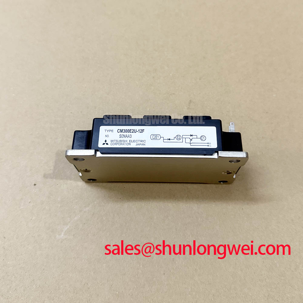
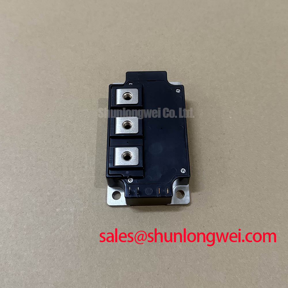
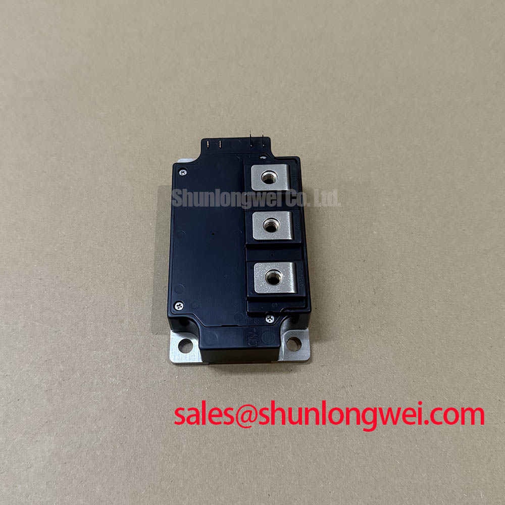
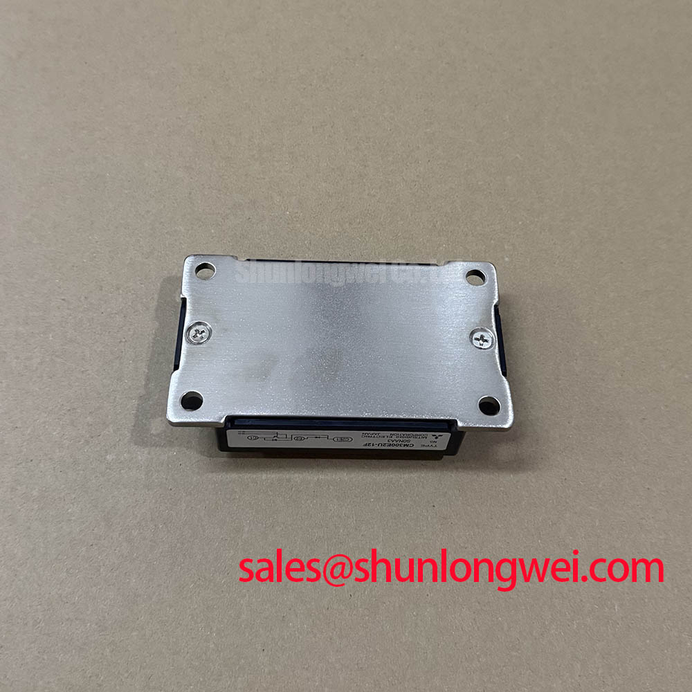
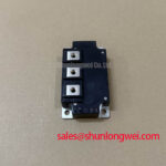
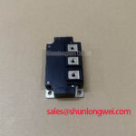
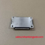
Begin incoming inspection with the module isolated from all power sources: check the markings, inspect the terminal housing for visible damage, and compare the required voltage and current ratings with the drive documentation before applying any test signal. For the Mitsubishi Electric CM300E2U-12F, the official ratings supplied for this product are shown below.
| Parameter | Official Specification |
|---|---|
| Collector Emitter Voltage, VCES | 600 V |
| Collector Current, IC | 300 A |
| Power Dissipation per Element, PC | 1040 W |
| IGBT Junction to Case Thermal Resistance, Rth(j-c) | 0.12 °C/W |
| Short Circuit Withstand Time, tsc | 10 µs at VCC = 400 V and VGE = 15 V |
These are device ratings, not a complete inverter operating prescription. The actual switching frequency, DC link voltage, gate drive conditions, cooling arrangement, overload profile, and protection coordination must be checked against the complete equipment design. A heavy duty variable frequency AC motor drive may evaluate this module in its inverter bridge, but compatibility depends on the original circuit topology and the surrounding gate driver, snubber, busbar, cooling, and protection hardware.
For a cold-state bench check, use an ESD-controlled workstation and a meter with the test leads verified against a known-good reference. Confirm terminal identity from the applicable Mitsubishi Electric documentation before connecting the instrument. A resistance or diode-mode reading can help identify an unexpected short circuit or an open measurement path, but it does not establish rated blocking capability, switching performance, or semiconductor health under load. Do not infer a pass or fail decision from an isolated meter value without comparing the complete terminal network and the original service condition.
💡 Bench Tip: Keep the module disconnected from the DC link and gate driver during static testing, then record the cold-state readings and terminal polarity before installation.
Transient Dynamics and Electrical Design for Suppressing Cres Induced Gate Voltage Spikes
In a high-voltage inverter, collector-to-gate coupling and common-mode movement can disturb a gate signal during the opposite switch transition. The CM300E2U-12F data supplied here confirms a 600 V VCES rating and a short-circuit withstand condition of 10 µs at VCC = 400 V and VGE = 15 V; it does not define a universal gate voltage, negative bias, active Miller-clamp circuit, or driver layout for every installation.
As a Design Consideration, a dedicated low-impedance gate driver with an active Miller clamp can reduce the opportunity for a rapidly changing collector voltage to raise the off-state gate potential. A negative gate bias may also be evaluated where the driver manufacturer, insulation system, and module documentation permit it. The proposed negative range in the application brief is not an official CM300E2U-12F parameter, so the system designer should verify the allowable gate-emitter limits from the original device documentation before applying any negative bias.
Keep the power commutation loop and gate-drive return path physically distinct, with the shortest practical routing between the driver and the module terminals. The control reference should return directly to the intended emitter reference rather than sharing a high-current path that carries switching current. Clearance and creepage around the high-voltage terminals must be established from the working voltage, pollution environment, insulation category, and applicable equipment standard. A generic spacing value cannot be assigned to this module without those system conditions.
During troubleshooting, inspect the gate-emitter waveform at the module terminals with a suitably rated differential probe. Compare the off-state excursion, turn-on delay, turn-off behavior, and common-mode movement against a known-good phase leg. If a pulse appears only when the opposite switch changes state, investigate parasitic coupling, driver return inductance, clamp timing, and probe connection before attributing the issue to the IGBT itself. Minimize parasitic loop inductance to suppress inductive overshoot, then verify the peak voltage against the DC-link boundary during controlled switching tests.
Benchtop Waveform Tuning for Multi-Module Parallel Current Sharing
Parallel operation requires more than connecting identical power terminals. The positive temperature coefficient commonly associated with IGBT conduction can support steadier static current sharing, but dynamic sharing remains strongly affected by gate-loop impedance, propagation delay, stray inductance, device temperature, and the physical symmetry of the busbar. The CM300E2U-12F official data supplied here specifies 300 A IC; it does not state a guaranteed parallel-current allocation for a particular assembly.
As an Engineering Recommendation, use symmetrical power paths and matched gate-drive routing when multiple modules are evaluated in parallel. Each gate loop should have a comparable physical path, return arrangement, and driver interface. The engineer should measure collector current and gate-emitter voltage on each parallel leg rather than assuming that equal cable length alone provides equal dynamic behavior. Any imbalance during turn-on or turn-off should be reviewed alongside the gate threshold behavior, driver output impedance, busbar geometry, and thermal distribution.
Dead-time must be selected by the system designer after measuring the complete driver and power-stage delays. It must prevent simultaneous conduction of complementary switches while avoiding excessive diode conduction and unnecessary recovery stress. The phrase “dead-time buffer” therefore describes a measured design requirement, not a fixed CM300E2U-12F specification. Interlock logic should remain effective during processor reset, driver undervoltage, emergency stop, and loss of a control signal.
For a benchtop waveform review, begin with a low-energy DC link and a controlled load. Capture both complementary gate signals, the switch-node voltage, and the current in each parallel path. Increase operating stress only after confirming that the gate signals retain the intended timing and that no unexpected pulse is produced during commutation. In regenerative braking or a large braking-resistor circuit, the DC-link rise and chopper switching conditions should be checked separately from the motor inverter leg. The resistor, fuse, chopper device, and control threshold form a system whose energy absorption capability cannot be inferred from the IGBT current rating alone.
The linked CM300DXDX1-24A may be reviewed as a separate cross-reference candidate when the original equipment documentation identifies a compatible electrical and mechanical interface. It should not be treated as an automatic substitute; voltage class, current rating, terminal arrangement, gate behavior, thermal path, and protection settings require a documented comparison.
Thermal Electrical Optimization and Reinforced Insulation Barrier Integrity
The official 1040 W PC value and 0.12 °C/W Rth(j-c) value are important inputs for the thermal design, but they do not by themselves establish the final junction temperature. Case temperature, interface condition, switching losses, conduction losses, airflow, heatsink structure, and transient duty all influence the result. The thermal interface should be inspected for full contact, contamination, uneven pressure, and mechanical distortion. General thermal-interface guidance is available in this reference on thermal grease and phase-change materials for heatsink coupling.
Reinforced insulation performance, dielectric withstand, and common-mode transient immunity must be verified from the module documentation and the complete drive assembly. The proposed values of greater than 5 kV isolation and greater than 100 kV/µs CMTI are not among the official CM300E2U-12F parameters supplied here and must not be presented as product guarantees. The integrator should confirm the insulation system, terminal geometry, creepage, clearance, pollution degree, altitude requirements, and the actual isolator or gate-driver ratings used around the module.
When a gate pulse appears during a high-voltage transition, inspect the control reference and isolated-driver supply at the same time as the gate-emitter waveform. Common-mode ground bounce can make a clean logic command appear abnormal at the power device. Cable shields, chassis bonding, isolation barriers, and return-current paths should be assessed as one system. A single disturbed waveform does not prove a failed module; repeat the measurement with a verified probe connection and compare the signal path with the inactive or known-good phase.
For a heavy-duty variable frequency AC motor drive, the service engineer should also inspect the DC-link capacitor connections, braking chopper loop, phase-leg busbar, and heatsink contact after a fault event. The broader relationship between inverter switching, renewable-energy conversion, electric-drive duty, and industrial power stages is discussed in Industrial Applications. That material provides application context, while the final insulation and thermal decision remains dependent on the actual equipment construction.
Circuit Protection and Reliability with Thermal Time-Constant Evaluation
The short-circuit rating must be treated as a controlled protection interval, not as an allowable continuous overload condition. For this device, the supplied official condition is 10 µs at VCC = 400 V and VGE = 15 V. The protection circuit should detect the abnormal current, block the gate command, coordinate the fault response, and limit repetitive fault exposure. Desaturation detection, current sensing, soft turn-off, driver undervoltage handling, and fault interlock are system functions that require validation on the completed drive.
Thermal evaluation should combine the official junction-to-case resistance with the heatsink path and the transient response of the real mounting assembly. For a pulsed overload, the engineer can use a multi-RC thermal model to estimate the temporary junction rise from the measured loss waveform, then compare the calculated junction temperature with the permitted device and system limits. This is an Engineering Calculation only when the loss profile, thermal impedance data, case temperature, and model assumptions are documented; the single steady-state Rth(j-c) value cannot replace transient thermal data.
Fast semiconductor fuses can limit fault energy when correctly coordinated with the power circuit. Their voltage rating, interrupting capability, clearing time, and I²t characteristic must be compared with the module short-circuit response and the DC-link fault energy. The reference on high-speed semiconductor fuses explains the protection principle, but it does not establish a fuse selection for this particular assembly. The final choice should be verified through the equipment protection study and controlled fault testing.
After a trip, record the gate command, driver fault output, DC-link voltage, phase current, heatsink temperature, and fuse condition before replacing the module. Inspect the terminal area and thermal interface, then repeat static checks only after the circuit has been fully discharged. A low-resistance reading may indicate damage, contamination, or an attached circuit path, so isolate the relevant terminals and compare the result with the documented terminal configuration. This approach separates an electrical overstress event from a driver, busbar, cooling, or protection fault without assigning an unsupported single cause.