



Content last revised on September 11, 2026
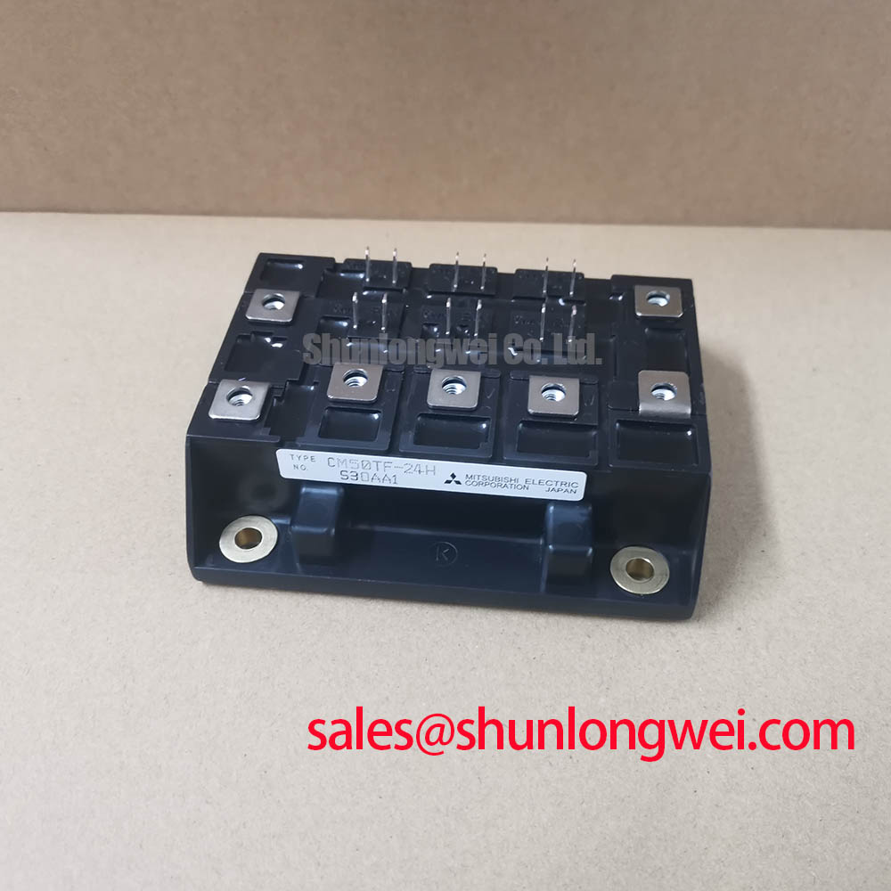
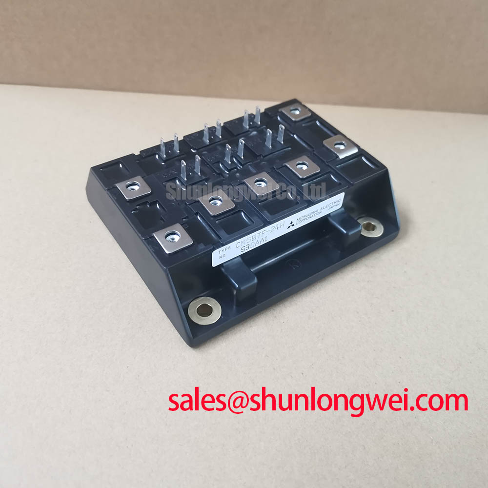
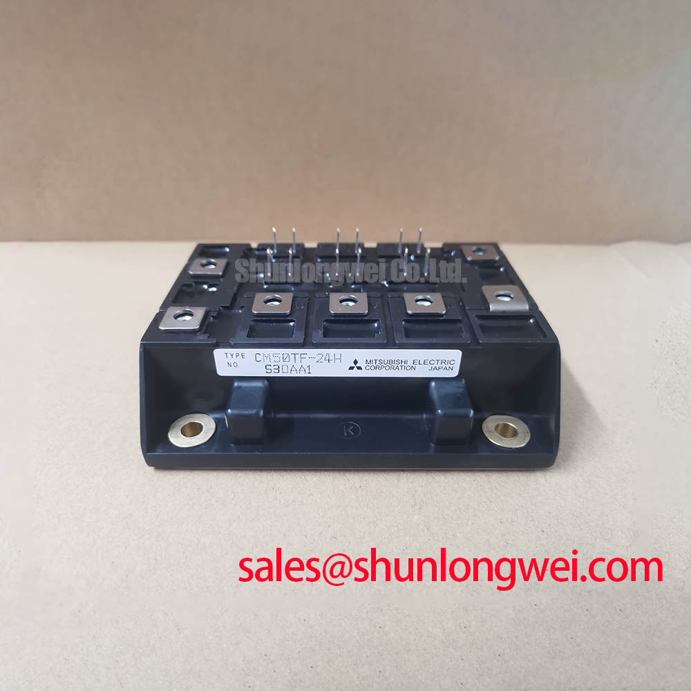
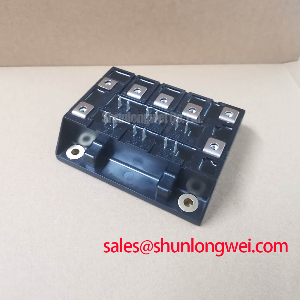
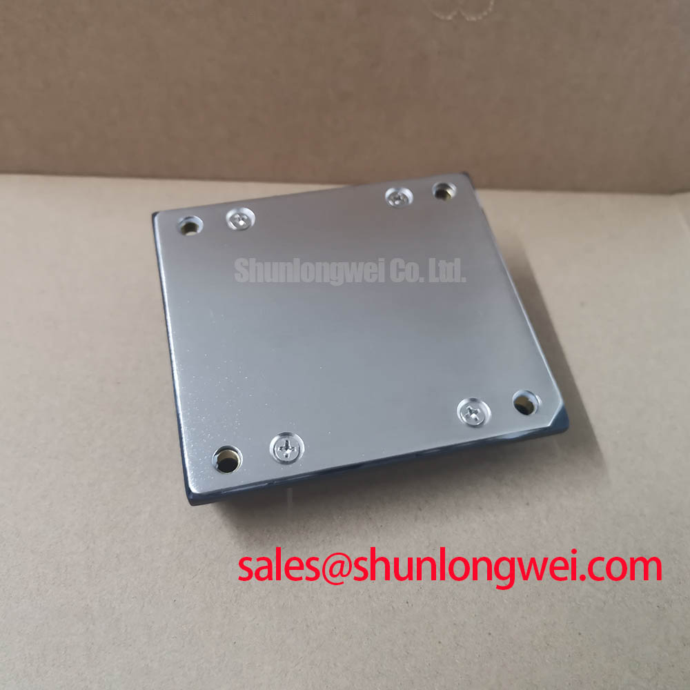
CM50TF-24H Mitsubishi Electric 1200V 50A IGBT Module
Confirm the nameplate rating, inspect the module housing and terminals, then perform a controlled cold-state impedance check against a known-good reference before energizing the assembly. The CM50TF-24H is a Mitsubishi Electric IGBT module with an official rated voltage of 1200.0 V, an official rated current of 50.0 A, and a module-style package. These values identify the basic electrical class, but they do not replace the complete manufacturer datasheet, switching conditions, thermal limits, gate-drive requirements, or circuit protection review.
| Parameter | Official Specification |
|---|---|
| Manufacturer | Mitsubishi Electric |
| Model | CM50TF-24H |
| Rated voltage | 1200.0 V |
| Rated current | 50.0 A |
| Package | Module |
For equipment repair, the voltage and current ratings should be checked against the actual DC-link voltage, load profile, switching frequency, cooling arrangement, fault-clearing response, and repetitive transient environment. A 1200.0 V rating and a 50.0 A rating are official device-class specifications; they are not a blanket approval for every operating point in a commercial string inverter or micro-grid energy-storage converter.
Preventing Spurious Faults: High-Altitude Cosmic-Ray and SEB Considerations for CM50TF-24H
When a converter is installed at elevated sites, begin the review with the measured DC-bus operating range rather than applying a generic altitude multiplier. Terrestrial neutron exposure and other high-energy particle effects can be relevant to high-voltage power semiconductor reliability, but a product-specific Single Event Burnout probability or FIT value requires an authoritative device study, defined test conditions, and a validated system model. No such field failure rate should be inferred from the 1200.0 V nameplate rating alone.
Design Consideration: At sites above approximately 2000 m, system engineers should reassess bus-voltage headroom, insulation coordination, cooling performance, creepage and clearance, and the protection response during abnormal switching events. The final derating policy should be established from the applicable insulation standard, inverter safety requirements, manufacturer data, and site qualification testing. Layout spacing should be treated as a system-level insulation decision, with contamination, enclosure environment, altitude, working voltage, and transient overvoltage included in the assessment.
For field troubleshooting, isolate the DC link, follow the equipment discharge procedure, and record whether the reported fault appears during startup, steady conduction, switching transitions, or a high-load event. Inspect the gate-drive waveform, collector-emitter voltage, desaturation or overcurrent protection timing, and the physical condition of the module and bus connections. An unexplained short circuit may involve electrical overstress, gate-drive malfunction, commutation behavior, cooling loss, or an external protection failure; it should not be assigned to cosmic-ray exposure without supporting analysis.
CM50TF-24H Operational Boundaries: Evaluating Common-Mode Transient Immunity
The CM50TF-24H product information supplied for this page confirms the module’s 1200.0 V voltage class, 50.0 A current class, and module package, but it does not establish a reinforced isolation voltage, an isolated-driver CMTI rating, or a 100 kV/µs immunity specification for the complete inverter. Those figures must be verified from the relevant gate-driver, isolation, and system documentation before they are used in a compliance or protection calculation.
During commissioning, observe the gate-emitter command and the power-switching node simultaneously with suitable differential and isolated measurement equipment. Common-mode displacement can couple through driver isolation capacitance, probe capacitance, heatsink structures, cable shields, and control-ground paths. If an unexpected gate pulse is suspected, compare the affected channel with the corresponding healthy channel during identical phase-angle or PWM conditions. Check driver supply stability, dead-time behavior, Miller plateau control, gate-loop routing, and the return path used by the gate signal.
For line-frequency or energy-storage topologies, the DC-link ripple profile should be measured under charging, discharging, regenerative, and grid-disturbance conditions. Ripple smoothing, phase-angle conduction control, and switching synchronization are system functions, so component selection alone cannot establish immunity. RC snubbers may reduce ringing when their values and placement are validated through waveform measurement; an arbitrary snubber value can increase loss, alter switching behavior, or stress the switching node.
For manufacturer-level semiconductor technology context, engineers can consult Mitsubishi Electric Power Semiconductors and High-Power Modules and the company’s Global Semiconductor Device Technologies resources. These references should be read alongside the exact module documentation and the selected isolated gate-driver data.
CM50TF-24H Circuit Protection and Reliability: Symmetrical Busbar Geometry
For a three-phase converter or bidirectional storage stage, current balance depends on both static and dynamic behavior. A positive temperature coefficient of on-state voltage can support passive current-sharing behavior in parallel semiconductor paths under suitable operating conditions, but that characteristic must be confirmed in the device data and evaluated across temperature, current, gate resistance, and switching state. It should not be treated as a substitute for matched electrical paths and protection coordination.
The practical design priority is symmetry. Keep the power paths, gate-drive paths, and return paths physically comparable, and avoid routing one channel through a visibly longer or more inductive loop. If the package provides auxiliary or emitter-related terminals, the system integrator should verify the exact terminal function from the original Mitsubishi Electric documentation before assigning a separate control return. Power-current routing and gate-signal routing should not share an uncontrolled return path.
Thermal verification should use measured case or heatsink temperatures, the actual cooling interface, and the manufacturer’s transient thermal impedance network where available. Pulse loading can produce a short-term junction-temperature excursion that is not visible in an averaged heatsink reading. The peak junction-temperature margin therefore needs to be assessed against pulse duration, repetition, conduction loss, switching loss, and the complete thermal path. A thermal interface layer should be uniform and free from trapped contamination, while mounting flatness and fastener procedure should follow the equipment and module documentation.
💡 Pro Tip: Disconnect the DC link and confirm the discharge state before removing any gate-drive or power connection, then verify the signal path with an oscilloscope before applying full bus voltage.
For a neutral cross-reference review, engineers may compare the published information for CM50DY-28H, while treating package geometry, terminal assignment, electrical ratings, thermal data, and gate-drive compatibility as items requiring independent verification rather than assuming direct interchangeability.
Field Diagnostics and Commissioning: Planar Busbar Geometry in CM50TF-24H Topologies
At commissioning, capture the collector-emitter voltage during turn-off at the module terminals, not only at a remote oscilloscope test point. The switching overshoot is influenced by DC-bus voltage, commutation current, switching rate, and stray inductance. In engineering terms, the inductive contribution rises with the product of stray inductance and current slew rate, so reducing the high-current loop and validating the resulting peak voltage is more reliable than selecting a layout target without measurement.
A laminated or closely coupled bus structure can reduce loop area, but the final geometry must be determined by mechanical insulation, current distribution, thermal clearance, service access, and the measured switching waveform. Do not assume a specific inductance value, including a sub-25 nH target, without a validated extraction or double-pulse test. The snubber capacitor, damping element, and physical placement should be selected from the observed ringing frequency, overshoot, pulse energy, and allowable loss.
During a double-pulse or controlled commissioning test, monitor gate voltage, collector-emitter voltage, current, heatsink temperature, and driver supply behavior together. Miller capacitance and plateau charge can couple a fast collector-voltage transition into the gate circuit, especially when the gate return shares power-current inductance. Active clamping or Miller control can be considered where the selected driver and protection architecture support it, but threshold, response time, and energy capability must be verified from the relevant circuit documentation.
Reverse recovery behavior in the freewheeling path also affects voltage overshoot and radiated noise. The diode’s recovery softness, commutation current, junction temperature, and loop geometry should be evaluated as a combined system rather than reduced to a single assumed softness factor. If EMI changes after replacing a power module, compare switching-node ringing, gate-loop waveforms, common-mode current, and heatsink or cable coupling. The technical discussion in Unlocking Efficiency in Industrial Drives provides additional background for relating switching behavior to industrial drive efficiency and layout decisions.
Before releasing a repaired commercial string inverter or micro-grid energy-storage assembly, verify insulation, protection interlocks, precharge behavior, gate-drive sequencing, current sensing, thermal alarms, and controlled-load operation against the original equipment procedure. The CM50TF-24H data confirmed here establishes the component’s 1200.0 V voltage class, 50.0 A current class, and module package; safe system operation still depends on documented circuit conditions and measured commissioning results.