Content last revised on October 8, 2026
Turn-Off di/dt Induced Vpeak Clamping and Snubber Capacitor Sizing
During an inverter repair, inspect the complete commutation loop rather than treating the module as an isolated switching element. Loose busbar joints, displaced capacitor connections, and altered conductor routing can change turn-off behavior even when the replacement carries the same designation. As a Design Consideration, place the relevant DC-link and snubber connections to minimize the current-loop area while preserving the equipment’s required electrical clearances.
An Engineering Calculation expresses the first-order relationship as Vpeak = VDC + Lσ × |di/dt|: stray commutation inductance adds a transient voltage during rapid current interruption. This relationship explains the mechanism, but it does not predict the complete waveform when ringing, diode behavior, and distributed capacitance are significant. Measure the collector-emitter transient with a suitably rated differential probe and a measurement arrangement that avoids introducing misleading pickup.
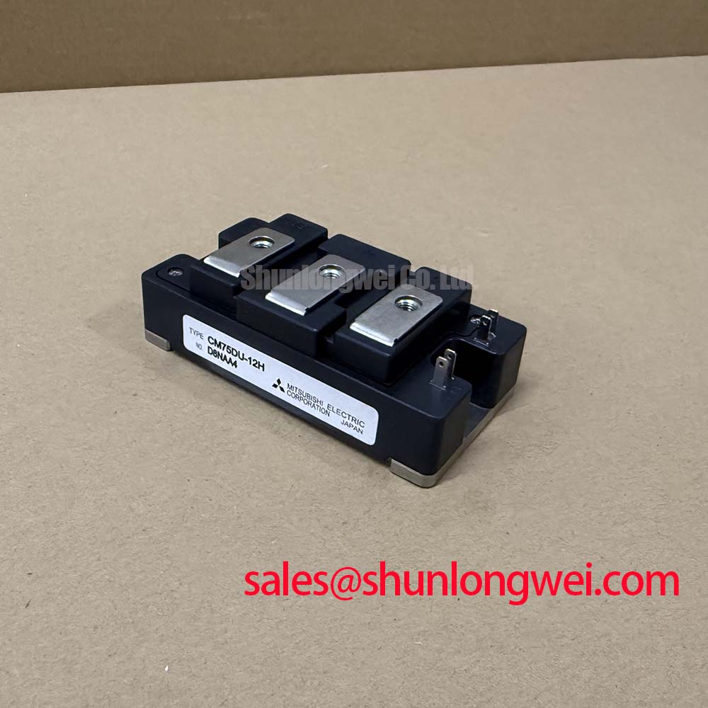
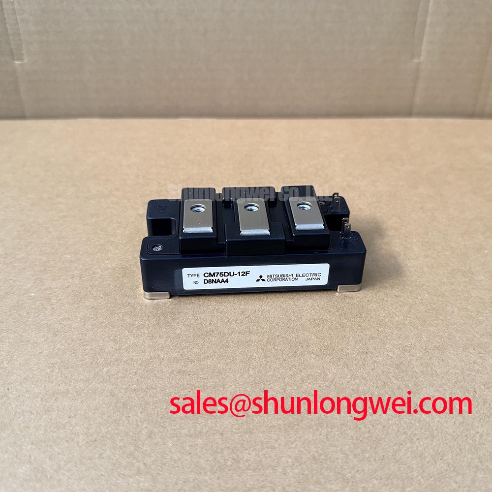
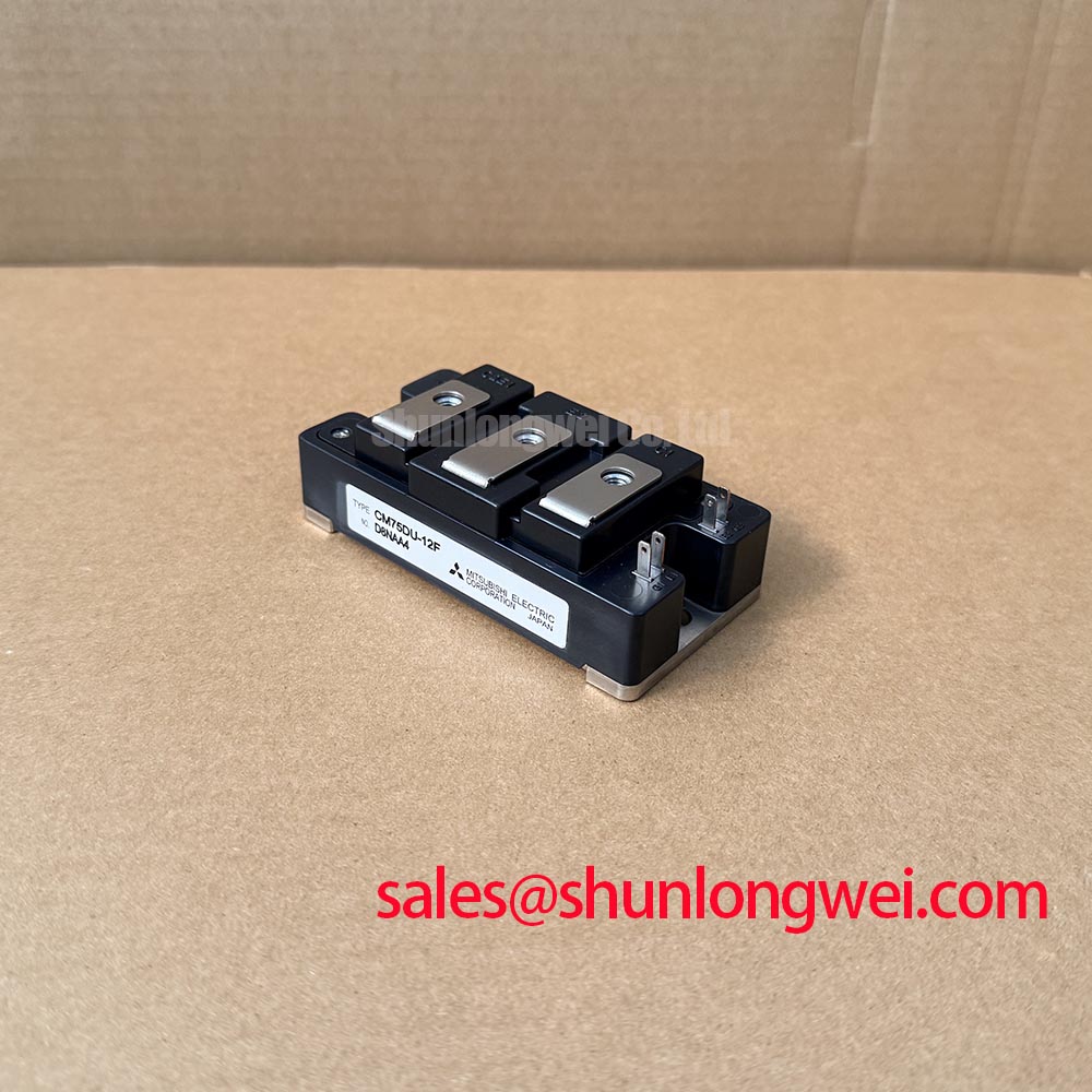
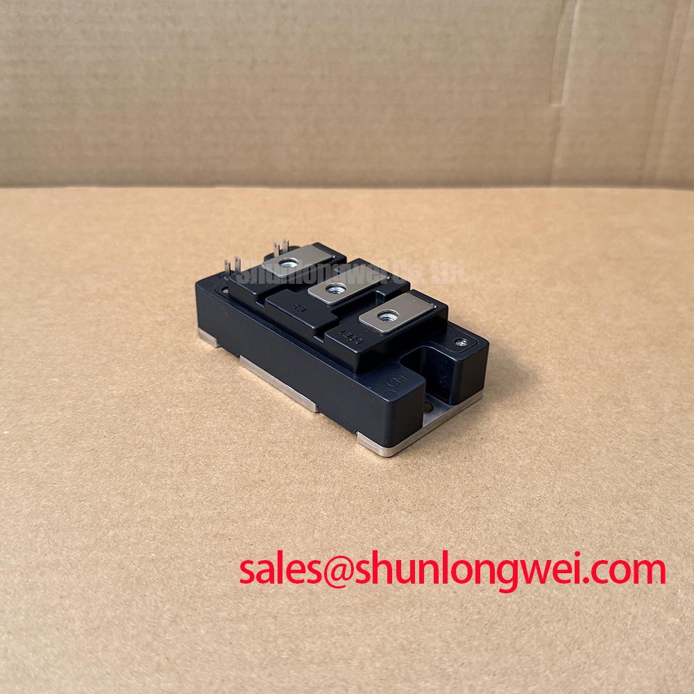
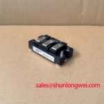
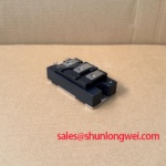
For the 600 V Mitsubishi Electric CM75DU-12F, designers should verify switching peaks against the applicable device limits throughout the intended operating envelope. A planar busbar arrangement can reduce parasitic inductance, but neither a universal inductance target nor a fixed voltage margin is established by the supplied product ratings. The acceptable geometry remains a system-level decision validated through measurement.
Snubber capacitance should likewise follow measured commutation behavior, allowable capacitor stress, damping requirements, and the associated losses. Increasing capacitance without checking pulse current and discharge paths can transfer stress elsewhere in the converter. When examining the wider power-stage assembly, the CM400HA-12E is a separate module reference for architecture comparison; its role and compatibility must be established from its own documentation, not assumed to be a rectifier or a direct replacement.
High dv/dt Cross-Conduction Shoot-Through Mitigation via Dedicated Miller Clamps
Before attributing an overcurrent trip to the CM75DU-12F, inspect the off-state gate waveform during complementary switching. As a Design Consideration, a rapid collector-voltage transition can couple current through the gate-collector capacitance and disturb the gate voltage. Whether that disturbance produces unintended conduction depends on the driver impedance, connection inductance, operating conditions, and device characteristics.
A dedicated active Miller clamp may help provide a low-impedance discharge path when supported by the selected gate driver. Designers should verify its activation behavior, physical connection, and compatibility with the module’s documented gate limits. Negative gate bias is another system-dependent option, not a requirement established by the 600 V, 75 A ratings; its value must come from the device limits and validated driver design.
Gate-driver sourcing and sinking capability should be evaluated against the required switching behavior and the relevant gate-charge information. External gate resistance affects switching speed, ringing, and losses, so a resistance selected for another module should not be carried over without evaluation. Check both gate-emitter and collector-emitter waveforms under controlled conditions, including the effect of temperature and current, before accepting a revised driver configuration.
For procurement comparisons, the CM15MD-12H can be reviewed as another Mitsubishi module designation, but shared branding does not establish interchangeability. Compare circuit configuration, terminal mapping, gate requirements, mounting dimensions, and thermal characteristics before considering any change to the equipment parts list.
Auxiliary Emitter Return Trace Separation for Rapid dv/dt Transients
Trace the gate-driver return from the driver board to the module using the original schematic and terminal drawing. The available confirmed specifications do not establish whether the CM75DU-12F provides a dedicated auxiliary emitter connection, so a Kelvin terminal must not be inferred from the product name. Where the documented terminal arrangement provides a separate control return, use that connection according to the original circuit design.
As a Design Consideration, impedance shared between a high-current emitter path and the gate-driver return can disturb the effective gate-emitter voltage during switching. Keep the control loop compact and avoid unnecessary shared routing with the power path, subject to the actual terminal layout and insulation requirements. If no separate return is available, evaluate the existing connection rather than assuming that a modified terminal arrangement is permissible.
For intermittent trips or oscillation, compare waveforms at the driver output and module terminals while checking connector seating, return continuity, and measurement pickup. A waveform difference may indicate wiring-related effects, but it is not a complete fault diagnosis. The Field Engineer’s Handbook provides supporting troubleshooting context; model-specific terminal limits and manufacturer instructions remain the controlling references.
Baseplate Thermal Grease (TIM) Layer Control & Heatsink Mounting Torque Optimization
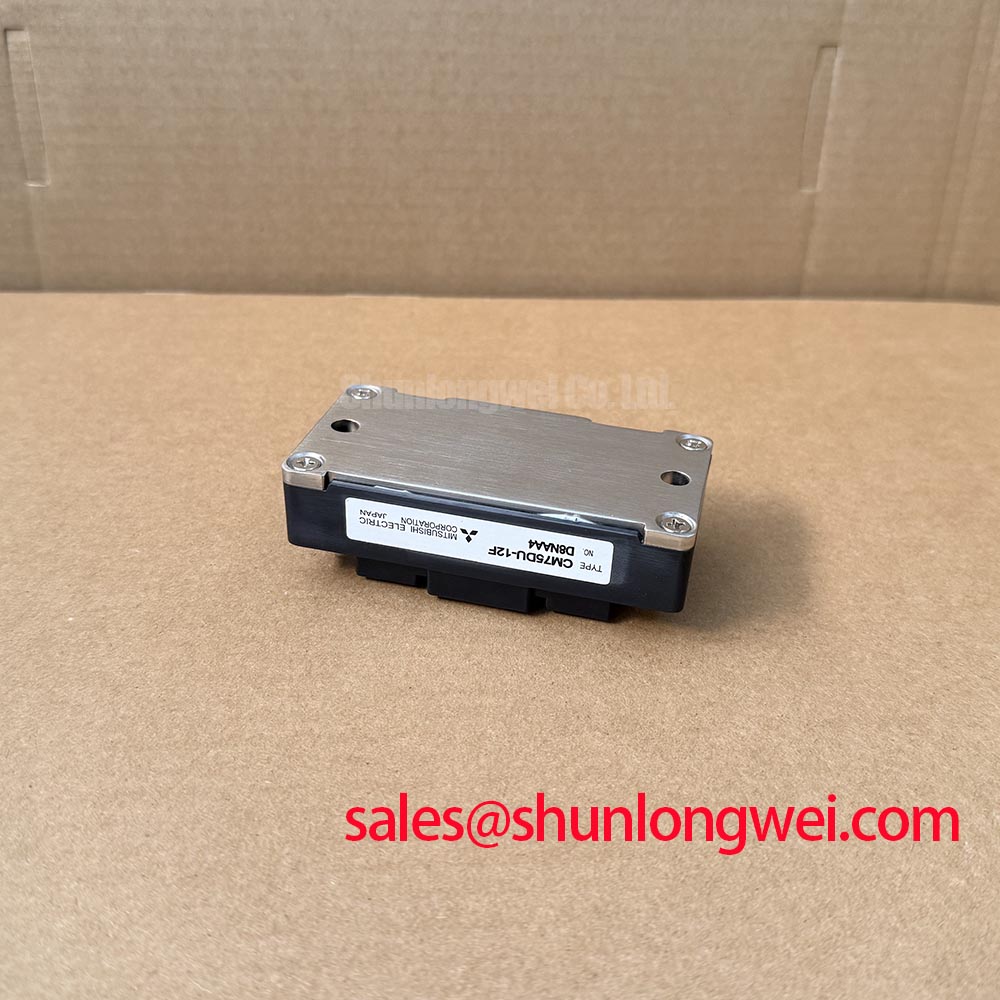
At removal, inspect the contact footprint for uneven thermal-interface coverage, contamination, or evidence of movement. Clean the heatsink using a method compatible with its finish, and check its contact surface against the applicable mounting requirements. As a Design Consideration, excessive interface material or incomplete coverage can impair heat transfer; neither a universal grease thickness nor a mounting torque can be assigned from the confirmed package description alone.
Apply the thermal-interface material and tightening sequence specified for the module and heatsink assembly. Avoid using fastener force to compensate for an unsuitable contact surface. The Mitsubishi Electric Power Semiconductors & High-Power Modules resource is the manufacturer reference point for obtaining applicable technical and mounting guidance.
Cooling maintenance should address blocked fins, restricted airflow, fan condition, and signs of interface deterioration. Set inspection intervals from equipment duty and observed trends rather than an assumed grease replacement calendar. In cabinets exposed to temperature changes, check for moisture and condensation before energization, and restore the enclosure’s intended environmental controls.
⚠️ Maintenance Note: Investigate a rising module-to-heatsink temperature difference under comparable load and ambient conditions before simply retightening fasteners or adding thermal grease.
After reassembly, verify terminal tightness using the specified torque procedure, confirm control wiring, and check that cooling components operate correctly. Where the equipment permits controlled loading, compare temperature trends with the recorded baseline before returning the converter to unrestricted service.