Content last revised on October 23, 2026
CM400DU-12F Cold-State Inspection Before Replacement
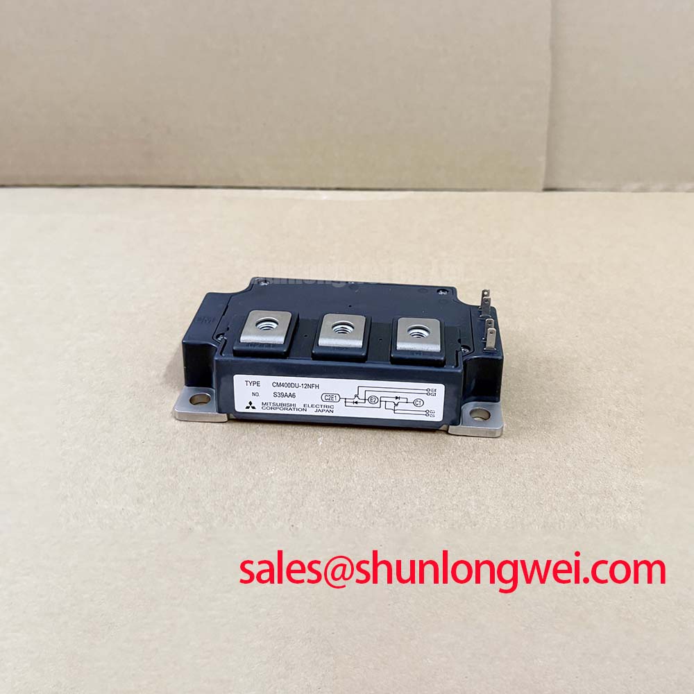
With the DC link discharged and its voltage verified, disconnect the gate-driver wiring and identify the collector, emitter, and gate connections from the terminal diagram before taking cold-state measurements. The Mitsubishi Electric CM400DU-12F has official specification ratings of 600 V collector-emitter voltage and 400 A collector current. Record the instrument range, module temperature, and probe polarity so incoming inspection results remain comparable with a known-good reference.
Use the multimeter’s diode function only on conduction paths identified in the circuit diagram, keeping the gate discharged through an ESD-safe handling procedure. Forward readings depend on test current and temperature; they are not equivalent to the official 1.6 V typical collector-emitter saturation voltage at 400 A and a junction temperature of 125°C. A handheld meter can support screening for abnormal conduction or leakage, but it cannot establish rated-current performance.
💡 Bench Tip: Discharge the gate through an ESD-safe procedure before each cold-state comparison, because retained gate charge can change the apparent collector-emitter reading.
Transient Dynamics & Electrical Design: Gate Drive Resistance Calibration when Replacing CM400DU-12F
Separate the external turn-on and turn-off gate-resistance paths on the legacy driver schematic before changing resistor values. As a Design Consideration, these paths influence different switching events: turn-on resistance affects current rise and commutation behavior, while turn-off resistance influences voltage overshoot and switching energy. Copying resistor values from a different module can change both device stress and driver loading.
Inspect the driver output stage, steering diodes, resistor placement, and return routing as one circuit. When integrating the CM400DU-12F, engineers should establish the permitted gate-voltage range and switching test conditions from its device documentation, then evaluate the existing driver against those requirements. Gate-voltage excursions should be measured at the module connections rather than inferred from the driver-board output.
For calibration, change one switching path at a time and compare collector-emitter voltage, collector current, and gate voltage under repeatable load conditions. A slower edge can reduce ringing while increasing switching loss; a faster edge can reverse that trade-off. The engineering acceptance criteria should therefore include measured overshoot, driver behavior, and thermal loading, rather than waveform appearance alone. Keep measurement loops compact and use probes suitable for the voltage and common-mode conditions.
A coordinated suppression network also needs distinct responsibilities. As a Design Consideration, a local RC snubber addresses switching-loop oscillation, while an MOV can address specified transient-energy events within its own operating limits. Neither automatically compensates for excessive commutation-loop inductance. Evaluate clamp voltage, pulse energy, repetition, and placement against the actual circuit. A system schematic containing a device such as CM150RX1-24A should identify its separate switching-stage role; its presence does not establish a shared gate-drive requirement or interchangeable function.
CM400DU-12F Operational Boundaries: Evaluating Symmetrical Busbar Geometry for High-Current Limits
Compare the resistance and inductance of each current path before attributing unequal module loading to semiconductor variation. As a Design Consideration, symmetrical busbar geometry, comparable joint condition, and consistent thermal interfaces help reduce differences between parallel branches. Matching only the visible conductor lengths can leave unequal contact resistance or different commutation-loop areas.
The official 400 A collector-current rating is a device boundary under its specified conditions, not a measurement of current sharing in an assembled converter. Likewise, the specified saturation-voltage point does not establish a positive temperature coefficient across every operating condition. Any proposed use of temperature-dependent saturation voltage for static balancing should be checked against the relevant output characteristics over the intended current and temperature range. Dynamic sharing additionally depends on driver timing and gate-loop impedance.
When reviewing an existing controller, distinguish PWM switching from any upstream phase-angle-controlled rectifier. Rectifier firing behavior and DC-link ripple determine the supply presented to the switching stage, but they are not functions established by the CM400DU-12F part number. Measure ripple under representative loading and examine whether current peaks coincide with uneven conduction or protection events. RC suppression should then address the identified transient path rather than serve as a substitute for correcting busbar asymmetry.
A replacement review involving CM300DY-12HE should compare the terminal arrangement, mounting outline, electrical ratings, gate requirements, and thermal characteristics independently. It should not treat a related designation as evidence of drop-in compatibility. For a utility-scale 1500 V central solar photovoltaic inverter, the CM400DU-12F’s 600 V rating rules out treating it as a direct full-bus switching replacement. Evaluation would require an established topology in which its individual blocking stress remains within the device limits, including switching transients.
Preventing Spurious Faults: Auxiliary Kelvin Emitter vs Main Power Emitter Guidelines for CM400DU-12F
Trace the driver return to its actual emitter connection before interpreting a noisy gate waveform. An auxiliary Kelvin emitter must be identified by the module’s terminal diagram; a small terminal or convenient emitter connection should not be assigned that function by appearance. This distinction is especially important when adapting an existing harness to a replacement module.
As a Design Consideration, shared emitter-path inductance can develop a voltage during rapid current change, altering the gate-emitter voltage seen by the switching device. Where a documented auxiliary emitter connection exists, its intended use is to separate the driver reference from the main load-current path. Otherwise, the return arrangement must follow the documented terminal configuration without inventing a dedicated internal sensing connection.
Investigate suspected false triggering by comparing the gate waveform at the module with the driver command and protection signals. Correlation with collector-current transitions can indicate common-impedance coupling, but probe pickup and driver-supply disturbance should also be checked. Route outgoing and returning gate conductors together where the assembly permits, keeping them away from high-current commutation paths. Required clearances remain dependent on operating voltage, insulation system, environment, and applicable equipment requirements.
The official isolation-voltage specification is 2500 V AC. That value is not permission to apply the same test indiscriminately across gate and emitter terminals or to repeat production withstand testing without an approved procedure. Incoming insulation checks should use the specified terminal grouping, test duration, and equipment procedure. Mitsubishi Electric’s power semiconductor and HVIGBT information provides manufacturer context, but this 600 V device should not inherit ratings or insulation claims from a different product family.
CM400DU-12F Thermal-Electrical Optimization: Thermal Time Constants and Peak Junction Practical Tuning
Capture the load-pulse duration, repetition pattern, and case-temperature history before estimating peak junction temperature. The official specifications include a 150°C maximum junction temperature, 1100 W collector power dissipation, and 0.11°C/W IGBT junction-to-case thermal resistance. These describe different limits and thermal relationships; the power-dissipation figure is not a continuous cooling capability available regardless of case temperature.
For an Engineering Calculation under steady thermal conditions, junction-to-case temperature rise is estimated by multiplying the relevant IGBT dissipation by its junction-to-case thermal resistance. Pulsed operation instead requires the device’s transient thermal impedance and the actual loss waveform. A multi-RC model can represent that response when its coefficients come from manufacturer data or a validated characterization; arbitrary time constants would produce an unsupported peak-temperature estimate.
As an Engineering Recommendation, include residual heating from earlier pulses when assessing repeated overloads. Case-temperature recovery alone does not establish that the junction has returned to its previous condition. Also distinguish IGBT conduction and switching losses from diode losses and other heat sources. The stated IGBT thermal resistance should not automatically be assigned to every internal conduction path.
During mounting, assess interface flatness, contact condition, and fastening requirements using the module’s mechanical instructions. Do not transfer press-pack disc-spring calibration or double-sided clamping procedures to this module without explicit mechanical support. Similarly, no diode surge-current rating or recovery interval should be inferred from the 400 A collector-current figure. For the relationship between switching overshoot and additional heating, Mastering Power System Dynamics provides supporting discussion of stray inductance and snubber design. After correcting the interface or suppression network, repeat the same load sequence and compare the measured case-temperature trajectory and calculated junction peak against the operating limits.