


Content last revised on September 21, 2026
Assembly Integrity & Layout Architecture: Implementing 6-Pulse and 12-Pulse Bridge Configurations for DD110F-160
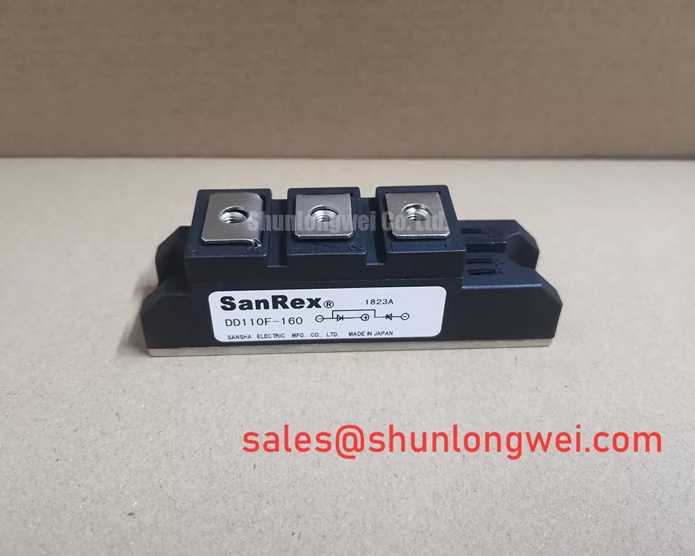
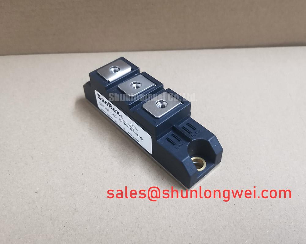
Before fitting the DD110F-160, verify the module marking against the service documentation, inspect the PowerBlock housing and terminals for transport or heat-related damage, and confirm that the isolated equipment is wired for the intended rectifier position.
The DD110F-160 Infineon diode module is rated at 1600 V and 110 A in a PowerBlock Module housing. These are Official Datasheet Specifications. The available factory information identifies this device as a diode module; it does not establish gate-trigger data, controlled firing-angle operation, reverse-recovery values, surge-current values, insulation ratings, mounting torque, fuse I²t limits, or thermal resistance values. Those properties must be confirmed from the original equipment documentation or the applicable manufacturer datasheet before a repair release or a new rectifier design decision.
| Parameter | Value | Specification Status |
|---|---|---|
| Product model | DD110F-160 | Official product identification |
| Manufacturer | Infineon | Official product identification |
| Repetitive voltage rating | 1600 V | Official Datasheet Specification |
| Rated current | 110 A | Official Datasheet Specification |
| Package | PowerBlock Module | Official Datasheet Specification |
| Device category | Diode Module | Official product classification |
A rectifier repair begins with topology confirmation, not with a visual match alone. In a six-pulse AC-to-DC bridge, diode modules occupy defined commutation paths between the AC phases and the positive or negative DC rails. A twelve-pulse arrangement normally combines two phase-shifted six-pulse bridge sections, with transformer and interphase arrangements determined by the complete power system. The 1600 V and 110 A ratings of the DD110F-160 establish electrical boundaries for evaluating its position, but they do not independently confirm suitability for any particular bridge output current, transformer secondary voltage, cooling arrangement, or fault duty.
For high-current green hydrogen electrolyzer DC power rectifiers, the visible DC output can be far greater than the current rating of one semiconductor location because system current sharing depends on bridge architecture, phase balance, transformer impedance, conductor resistance, and thermal conditions. Engineers should trace each power path from transformer secondary to DC bus, identify every parallel branch, and compare the installed module arrangement with the original schematic. Interphase transformer current balancing is a system function. It should not be assumed simply because two bridge outputs are connected in parallel.
Use short, symmetrical busbar paths where the mechanical layout allows. This is a Design Consideration: reducing loop inductance helps control commutation-related voltage excursions and promotes more repeatable current distribution. The system engineer should verify peak voltage at the installed module terminals under representative load and line conditions, then compare measured results with the 1600 V official voltage rating and the equipment’s approved transient-protection strategy.
A metal-oxide varistor network, where present in the original equipment, should be evaluated as part of the complete overvoltage-control assembly rather than as an accessory separate from the diode module. Its clamping behavior, energy capability, connection lead length, coordination with RC networks, and upstream protection must be selected and tested at system level. No MOV clamp voltage or energy value is established here for DD110F-160.
Terminal joints deserve the same attention as the semiconductor itself. Confirm that cable lugs, busbars, spacers, washers, and terminal orientation follow the original mechanical stack-up. A loose, tilted, or contaminated connection can raise contact resistance and produce localized heating that may be misinterpreted as a diode failure. The module mounting interface should be clean, flat, and consistent with the original heat-sink assembly process. Mounting torque and thermal-interface thickness are not supplied as official DD110F-160 parameters in the available data, so the equipment service procedure or manufacturer documentation should control those values.
⚡ Safety Interlock Note: Isolate all AC sources, lock out stored DC-link energy, and verify absence of voltage before disconnecting any rectifier busbar or module terminal.
Where a repair team is evaluating a different module family, compare circuit function, voltage class, current class, terminal arrangement, thermal interface, and protection coordination as separate checks. A linked reference such as DDB6U180N16RRP_B37 can support a documented comparison, but it is not an automatic replacement recommendation for DD110F-160.
Preventing Spurious Faults: Reverse-Recovery Behavior and Temperature Considerations for DD110F-160
In a line-frequency diode bridge, commutation transfers current from one conducting diode path to another as the AC phase relationship changes. This transition can interact with transformer leakage inductance, busbar inductance, snubber networks, and protection circuits. Diode reverse recovery behavior can influence transient current, voltage ringing, and conducted or radiated noise, but no official reverse-recovery peak current, recovery time, recovery charge, softness factor, or temperature coefficient is available in the supplied DD110F-160 specification set. Those values should not be estimated and presented as module data.
A practical commissioning approach is to capture terminal voltage and branch current with measurement equipment appropriate for the system voltage and available fault energy. Compare waveforms across equivalent bridge locations where the layout permits. Unequal commutation signatures may indicate differences in branch impedance, transformer balance, snubber condition, busbar geometry, connection integrity, or semiconductor behavior. A waveform alone does not establish one exclusive cause; it should be assessed alongside temperature observations, resistance checks performed safely off-line, and the original rectifier schematic.
Temperature remains relevant because semiconductor forward conduction and recovery behavior are temperature dependent in general. This is a Design Consideration, not an official temperature coefficient for this module. During loaded verification, engineers should monitor whether one PowerBlock location is persistently hotter than comparable positions operating under the same cooling and current-sharing conditions. If it is, inspect cooling-path contact, airflow or liquid-cooling performance, bolted joints, parallel-current paths, and transformer secondary balance before attributing the condition to the diode module alone.
For controlled rectifier systems containing thyristors in other positions, gate pulse amplitude, pulse duration, pulse-train strategy, reference-cathode routing, and firing synchronization must be verified according to the thyristor manufacturer’s documentation. The DD110F-160 is identified here as a diode module, so gate trigger current and gate trigger voltage do not apply as DD110F-160 product specifications. Mixing diode and thyristor diagnostic criteria is a common source of avoidable commissioning confusion.
Industrial rectifier assemblies may also include a separate front-end or complementary power stage. The TT570N16 reference may be reviewed when documenting related rectification-stage components, provided its circuit role and manufacturer ratings are independently checked. Component family names and voltage classes alone are insufficient for a replacement decision.
For background on common module arrangements and circuit topology terminology, engineers can consult Power Module Architecture & Topologies. System EMC compliance, however, is determined by the assembled converter, cabling, enclosure, filters, grounding, control circuits, and test configuration. A diode module is not independently represented as meeting whole-system EMC requirements.
Field Diagnostics & Commissioning: AC-to-DC Characteristics in DD110F-160 Topologies
Commissioning a DD110F-160 diode bridge requires a clear distinction between an uncontrolled diode rectifier and a phase-controlled thyristor rectifier. A diode bridge conducts according to the instantaneous AC voltage relationship and load current path; it does not accept a firing-angle command. Therefore, an alpha range from zero to one hundred fifty degrees is not a controllable transfer characteristic of the DD110F-160 itself. If the host rectifier uses phase-angle control, that behavior belongs to separate controlled semiconductor positions and their gate-drive system.
Start with an off-line topology check. Confirm phase labels, DC positive and negative rails, parallel links, current sensors, fuses, transient suppressors, and measurement reference points against the original drawing. With the system energized only under approved procedures, compare AC phase balance and DC output ripple against known-good commissioning records where available. A low DC output, excessive ripple, or unexpected input current distortion can arise from several sources, including supply imbalance, transformer issues, open protection devices, poor interconnections, control faults in adjacent thyristor sections, cooling interlocks, or a damaged rectifier path.
The rated 110 A current is an official module rating, not a complete electrolyzer output-current prediction. Actual current capability in a high-current DC rectifier depends on topology, conduction sharing, transformer loading, cooling, ambient conditions, protection coordination, and the manufacturer-approved operating envelope. When integrating or servicing equipment, designers should verify the measured current through each DD110F-160 location under controlled load conditions rather than inferring equal sharing from a common DC bus.
Reactive-power demand and input power factor also belong to the complete rectifier arrangement. In a diode bridge, displacement and distortion effects are influenced by the supply, transformer impedance, DC smoothing reactor, load profile, harmonic filtering, and the number of pulses. In a controlled bridge, firing angle adds another system variable. These characteristics cannot be assigned to the DD110F-160 from its 1600 V, 110 A and PowerBlock identification alone.
💡 Pro Tip: Keep corresponding phase busbars geometrically consistent where possible, then validate commutation voltage and branch-current balance with properly rated measurements under the actual system operating conditions.
For engineers working through application-level electrical margins, service testing, and industrial conversion equipment context, the Industrial Applications resource provides related power-semiconductor integration material. It should be used as supporting context alongside the original rectifier schematic and the official documentation applicable to the installed module.
Transient Dynamics & Electrical Design: I2t Fault-Protection Coordination for DD110F-160
Fault protection coordination must begin with verified withstand data for every component in the fault path. The supplied DD110F-160 information confirms only its 1600 V voltage rating, 110 A current rating, and PowerBlock package. It does not provide an official semiconductor surge-current rating, non-repetitive forward-current rating, fuse I²t withstand rating, or permitted fault-clearing energy. A fuse selection cannot therefore be calculated responsibly from the available module parameters alone.
In a DC rectifier fault, the available fault current and clearing behavior are determined by the AC source, transformer impedance, line impedance, reactor saturation behavior, DC bus capacitance where fitted, parallel bridge paths, cable inductance, and fuse characteristics. A semiconductor fuse’s pre-arcing and total-clearing I²t must be coordinated against documented module withstand capability, while its voltage rating, interrupting rating, and mounting arrangement must suit the complete equipment. The fuse manufacturer’s curves and the original rectifier protection study should govern that assessment.
Do not infer a safe short-circuit interval from the module’s normal 110 A current rating. Normal current capability and fault-energy survival are different conditions. If historical fuse data are unavailable, a repair engineer should identify the existing fuse part number, verify its data sheet, inspect the fuse holder and conductor condition, and escalate any uncertainty to the equipment designer or qualified protection engineer before energizing a high-energy rectifier.
Transient overvoltage during fault interruption should also be measured or evaluated as a system event. Minimize parasitic loop inductance in the fuse, busbar, suppression-network, and module connection paths to reduce inductive overshoot during current interruption. The final arrangement must be verified against the DC-link voltage, transformer conditions, actual fault-clearing behavior, and the official voltage boundary of 1600 V. No specific layout-inductance target or suppression setting can be assigned to DD110F-160 without the complete system data.
Power-semiconductor module manufacturers and industry sources provide broader information on module categories and integration practices; SanRex power semiconductor resources can be consulted for general industry context. For the installed DD110F-160 position, the release decision should remain tied to verified module ratings, original equipment drawings, documented fuse coordination, physical inspection, and controlled electrical testing.