Content last revised on September 10, 2026
DDB6U180N16RRP_B37 Operational Boundaries: Gate-Drive and Thermal Checks
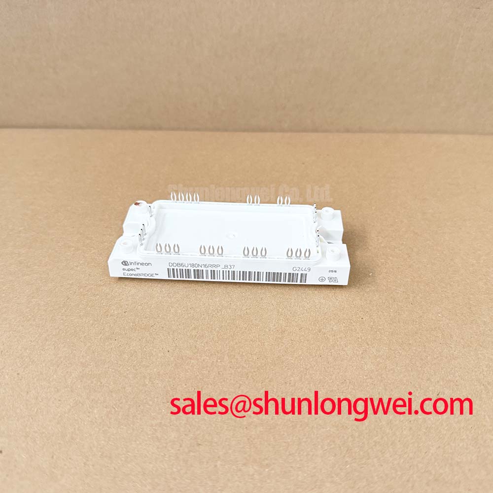
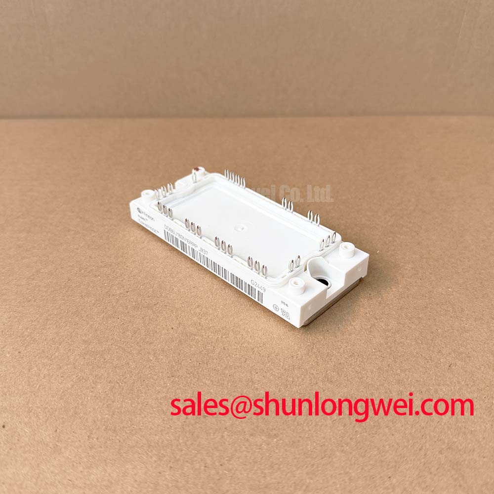
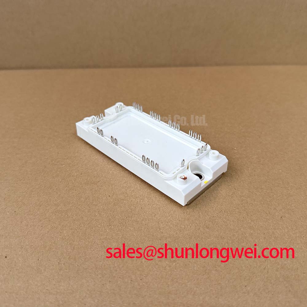
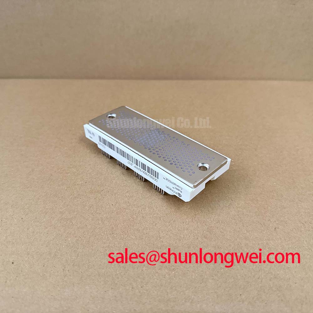
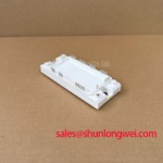
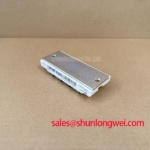
With the DC link discharged and isolated, verify the terminal identification, inspect the baseplate for flat contact surfaces, and confirm that the installed assembly matches the DDB6U180N16RRP_B37 electrical boundary before reconnecting power. This Infineon power assembly combines a rectifier bridge, a brake chopper stage, and an integrated temperature sensing element for equipment where AC input conversion, DC bus energy control, and thermal feedback must be assessed as one serviceable unit.
| Integrated Function | Official Datasheet Specification | Engineering Relevance |
|---|---|---|
| Rectifier bridge | VRRM = 1600 V | Repetitive peak reverse voltage rating for the bridge rectifier section. |
| Brake chopper | VCES = 1200 V | Collector emitter voltage rating for the integrated IGBT brake chopper section. |
| Temperature sensing | NTC = 5.0 kΩ at TC = 25°C | Reference resistance for temperature feedback verification at the specified case temperature. |
The first commissioning check is to separate the functions of the assembly during measurement. The rectifier bridge should be assessed from its AC and DC terminals, while the brake chopper section should be assessed through its designated power and control connections. The official bridge rating is 1600 V VRRM, while the brake chopper IGBT is rated at 1200 V VCES. These are distinct ratings for distinct internal functions and should not be treated as interchangeable voltage limits.
For a repair engineer examining a medium frequency induction melting or hardening furnace supply, the control board, gate driver output, DC link layout, brake resistor path, and chopper terminals should be checked together. A gate signal that is distorted by a poor return path, an unstable driver supply, or a loose control connection can alter switching behavior even when a static semiconductor measurement appears acceptable. The available official data supplied for this part does not define gate pulse rise time, gate holding current, multipulse firing limits, gate resistance, fuse I2t coordination, or terminal torque. Those values should therefore be verified from the original equipment documentation and the applicable Infineon documentation rather than inferred from another module family.
Design Consideration: the gate driver loop should be kept physically compact and paired with its return path so that parasitic inductance does not create unwanted gate voltage movement during switching. This becomes particularly relevant when the brake chopper diverts regenerative energy and the DC link is already experiencing a fast voltage transition. A measurement at the gate emitter reference and a simultaneous measurement of collector emitter voltage can help the system engineer determine whether an observed event is related to gate control, power loop inductance, or external braking circuitry.
A metal oxide varistor network, where used by the equipment designer, should be evaluated as a coordinated system element rather than regarded as a substitute for correct braking control. Its placement, energy capability, and clamping behavior must be checked against the actual bus architecture and measured transient conditions. The brake resistor and its switching path also need inspection for insulation condition, terminal security, and signs of heat exposure.
💡 Pro Tip: Keep the brake chopper power loop and its gate return physically close and verify switching margins with a controlled double pulse test before returning the furnace power unit to production.
When a different power module is being evaluated for an existing design, pinout, voltage class, thermal interface, driver compatibility, and protection behavior require independent verification. A device such as TT570N16 can be reviewed as a separate sourcing reference, but it should not be assumed to be electrically or mechanically interchangeable with the DDB6U180N16RRP_B37 without a documented system level comparison.
Assembly Integrity & Layout Architecture: Ensuring Uniform Heatsink Contact Pressure for DDB6U180N16RRP_B37
Before installation, clean the mating heatsink surface and inspect it for burrs, scratches, raised contamination, or evidence of prior uneven clamping. The DDB6U180N16RRP_B37 contains multiple power functions, so poor thermal contact can affect bridge rectification, brake chopper duty, and the relationship between actual case temperature and the NTC feedback signal. The integrated thermistor is specified at 5.0 kΩ when TC is 25°C. This provides a defined reference point for checking the temperature monitoring path, but it is not a direct substitute for a calibrated thermal characterization of the full cooling assembly.
Design Consideration: apply thermal interface material as a controlled, continuous layer that fills surface irregularities without creating excessive thickness. The clamping sequence should progressively distribute pressure across the baseplate. Fasteners, washer arrangements, mounting holes, tightening torque, and any disc spring arrangement must follow the module documentation and the equipment manufacturer’s installation procedure. No official mounting torque, screw size, baseplate dimension, or thermal resistance value is supplied here for this exact model, so those figures should not be substituted from visually similar modules.
After fastening, inspect whether the module sits flat against the heatsink and whether the power terminals remain mechanically unstressed. Busbars that pull sideways on a terminal can introduce assembly stress and reduce long term connection stability. Where dual sided cooling plates or clamped bus structures are used in a furnace power supply, the pressure relationship should be checked as a complete mechanical stack. The objective is even contact and repeatable fastening, not the application of an assumed force value.
Thermal verification should combine the NTC signal with operational measurements. At a controlled load condition, compare the temperature feedback trend with the cooling system response, fan or pump operation, heatsink cleanliness, and the temperature pattern of neighboring power components. A rapidly changing NTC value may reflect a real thermal event, an intermittent sensor connection, or a measurement circuit issue. Inspect the sensor wiring and controller input before attributing the result to the power assembly itself.
For engineers reviewing related DC supply stages, TD210N12 is a relevant separate component reference for topology review. Its presence in a system does not establish compatibility with this integrated Infineon assembly; the original schematic, terminal arrangement, and operating waveforms remain the controlling evidence.
DDB6U180N16RRP_B37 Operational Boundaries: Dynamic Voltage Overshoot and RC Damping
The 1600 V VRRM bridge rating should be checked against the actual line derived DC bus, line disturbances, commutation behavior, and measured transient peaks at the module terminals. The 1200 V VCES rating applies to the brake chopper IGBT and requires its own evaluation against the DC link voltage and braking event waveform. A brake resistor circuit can operate only as intended when its switching device, command signal, wiring loop, and energy handling path are all working together.
Design Consideration: minimize the inductive area formed by DC link capacitors, the brake chopper terminals, the braking connection, and associated busbars. This reduces the tendency for turn off overshoot caused by changing current. Engineers should verify peak voltage at the actual module terminals during switching tests, because a measurement point several centimeters away can conceal the local transient that the semiconductor experiences.
An RC damping network can be appropriate in some system topologies, but its resistance, capacitance, voltage capability, pulse handling, and location are determined by the measured resonance and thermal duty of the equipment. There is no official RC snubber value provided for the DDB6U180N16RRP_B37 in the available product data. A system integrator should therefore characterize the oscillation using suitable high bandwidth differential measurement equipment and validate damping behavior under the intended operating conditions.
Series saturable reactors, if present in an existing induction heating power source, should likewise be retained or changed only after waveform validation. Their effect on current rise, fault response, and commutation conditions depends on the complete converter structure. The same principle applies to DC bus film capacitors and MOV devices. A component value that performs acceptably in one furnace cabinet may not produce the same result after changes to cable routing, busbar geometry, cooling arrangement, or switching sequence.
For broader comparison of switching technologies and the design factors that accompany faster power transitions, see Wide Bandgap Revolution. That technical reference is useful when reviewing system level switching behavior, while the DDB6U180N16RRP_B37 itself must remain within its documented silicon based bridge and brake chopper operating boundaries.
Field Diagnostics & Commissioning: Reverse Recovery Evaluation in DDB6U180N16RRP_B37 Topologies
During a controlled recommissioning sequence, observe the AC input, rectified DC link, brake chopper command, collector emitter waveform, and NTC feedback as separate channels. This method avoids treating a DC bus disturbance as proof of a single component fault. In a rectifier bridge, reverse recovery behavior can contribute to commutation current peaks and conducted noise, while in the brake chopper path, switching transitions can interact with wiring inductance and the condition of the DC link capacitors.
The available official parameters for this model identify the bridge voltage rating, brake chopper voltage rating, and NTC reference resistance. They do not provide reverse recovery peak current, reverse recovery time, reverse recovery charge, soft recovery classification, junction to case thermal resistance, surge current capability, temperature coefficient curve, or fuse coordination values. Those characteristics should not be estimated from the ratings alone. If reverse recovery performance is important to a repair decision, engineers should consult the applicable manufacturer documentation or capture commutation waveforms from a known stable unit using appropriate safety procedures.
A ringing waveform may indicate several possible conditions, including busbar inductance, capacitor degradation, a changed snubber network, measurement probe setup, or a gate drive timing issue. Compare waveform shape at equivalent operating points and verify the measurement reference path. If an abnormal temperature rise accompanies the waveform change, inspect cooling contact, controller behavior, brake resistor operation, and NTC continuity before replacing major assemblies.
For induction melting and hardening equipment, commissioning should begin at a controlled operating state determined by the machine manufacturer. Confirm that the rectifier produces the expected DC link behavior, that the brake chopper responds to the controller command, and that the NTC input is plausible relative to case temperature. The final acceptance decision should be based on measured voltage, current, temperature feedback, and switching observations from the complete installed system.