

Content last revised on September 10, 2026
Incoming Benchtop Inspection: COG/TAB Anisotropic Conductive Film Integrity
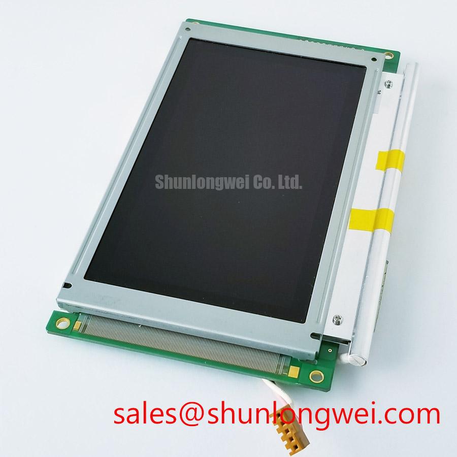
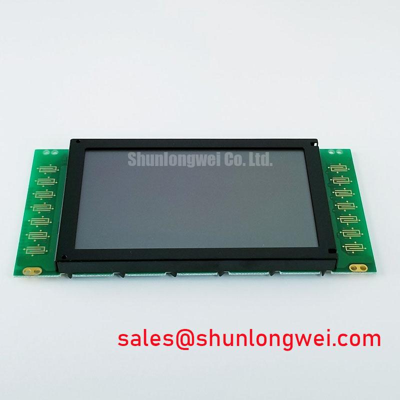
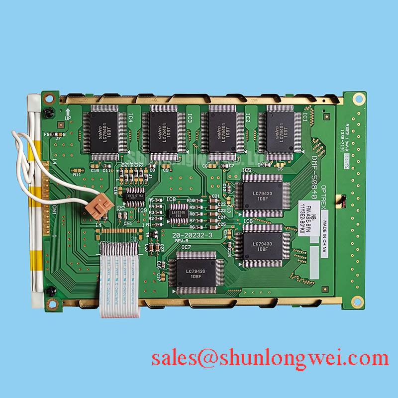
Begin the incoming inspection by checking the DMF-50840NB-FW module for frame distortion, exposed edge damage, connector contamination, and visible abnormalities around the display bonding area before applying power. This Kyocera / OPTREX product is identified as an Industrial Grade LCD/HMI Panel in a TFT-LCD Display Module package, with an official factory specification status provided for sourcing reference. The supplied factory data does not confirm panel resolution, active-area dimensions, interface type, supply voltage, backlight current, luminance, viewing angle, or operating temperature. Those values should be verified against the original equipment documentation and the applicable panel datasheet before installation.
Keep the module unpowered while examining the glass edge, flex connections, bonding zones, and connector housing under controlled bench lighting. COG and TAB bonding areas are mechanically sensitive, so avoid pressing the visible flex section or using a probe directly on the bonded edge. Look for lifted flex material, uneven contact pressure, cracks in the glass perimeter, contamination on the connector, and frame deformation that could change the mechanical stress applied during installation.
A practical primary-color inspection can be performed after confirming the system’s approved electrical conditions. Display red, green, and blue test fields separately, then observe whether the defect remains fixed in the same physical location or changes with the displayed color. A stationary line, column, or block can require inspection of the signal path, bonding area, and host timing configuration. A nonuniform dark region may also be associated with the backlight or optical stack rather than the COG driver connection, so the visual result should not be assigned to one cause without comparison testing.
A flashlight held at approximately a 45-degree angle can help distinguish a dark LCD region from a loss of illumination. If the area changes in appearance when viewed with oblique light while image content remains partially visible, inspect the backlight path and optical uniformity. If the image data itself is absent or distorted along a fixed line, compare the affected area with a known-good signal path and inspect the bonding edge for mechanical damage. This is a diagnostic method, not a factory acceptance limit for this model.
Temperature testing requires particular care. Liquid-crystal response can become slower in sub-zero environments, and a display that appears responsive at room temperature may show visible gray-to-gray transition elongation in a cold enclosure. The supplied information does not establish a rated operating range for this module, so any evaluation around −20°C to −30°C must be treated as a system-level design test rather than an official rating. If the equipment includes a heater strip, the integrator should control it from measured panel temperature and verify warm-up behavior without allowing localized heating to create optical gradients or mechanical stress.
For applications such as a high-voltage substation protection and SCADA dispatch console, the physical inspection should include the front bezel, mounting points, cable bend radius, and protective window clearance. The module’s suitability depends on the host enclosure, sealing method, vibration profile, and service access. The Ultimate Guide to Industrial TFT LCD Technology provides broader reference material for display selection and industrial integration checks.
Digital Display Interface Synchronization & Logic Power Rail Verification
The official data supplied for DMF-50840NB-FW does not identify the electrical interface as TTL RGB, LVDS, or another signaling standard. Do not connect a controller based only on the model designation. The system integrator should verify the required supply voltage, interface type, pin assignment, color depth, scan timing, and backlight control method from the original panel documentation before energizing the unit.
If the original system uses a 24-bit digital RGB bus, verify that the red, green, and blue data groups are mapped to the controller in the intended bit order. JEIDA and VESA conventions can arrange high-order color bits differently, and an incorrect mapping may produce incorrect color balance, posterization, or image patterns that resemble a damaged panel. If the host uses LVDS, confirm the transmitter mapping, lane order, clock position, polarity, and termination arrangement from the original equipment design rather than applying a generic cable pinout.
Power sequencing should be checked with an oscilloscope at the module connector. Confirm that the logic rail rises cleanly, that enable signals follow the host controller’s documented order, and that the display data clock does not begin outside the panel’s permitted startup window. The timing values required for this model are not included in the supplied factory parameter set. Values such as power-on rise time, reset delay, data hold time, and display-enable delay must therefore come from the applicable technical documentation.
When a screen shows split images, color swaps, unstable vertical content, or intermittent blanking, compare the clock and data waveforms at the panel connector with the known-good path. Check connector seating, ground reference continuity, cable orientation, controller configuration, and the relationship between the pixel clock and data transitions. An oscilloscope comparison is more reliable than assigning a single fault from the visual symptom. Temperature cycling should also be considered where the equipment operates in a wide ambient range, because cable resistance, connector contact behavior, and timing margin can shift with enclosure temperature.
For high-speed connections, the routing principle is to preserve a controlled return path, minimize unnecessary stubs, and maintain consistent pair geometry where differential signaling is used. A 100-ohm differential characteristic impedance may be a relevant design consideration for a compatible LVDS transmission path, but it is not an official electrical specification for this display based on the supplied information. The system designer must confirm the interface standard and validate signal integrity at the installed cable length.
💡 Pro Tip: Keep the display cable away from switching power loops and verify clock quality at the module connector after the cable, shielding, and enclosure are installed, not only on the controller bench.
Industrial EMI Noise Immunity, Chassis Shielding Continuity & Common-Mode Ferrite Chokes
A SCADA console positioned near variable-frequency motor drives can experience conducted and radiated interference through the display cable, chassis, DC supply, or protective earth arrangement. The display itself cannot be claimed to have independent compliance with an equipment-level EMC standard. EMC performance must be evaluated as part of the complete controller, cable, enclosure, power supply, and grounding topology.
Inspect the cable shield termination at both the display and controller ends according to the system grounding design. A shield that is connected through a long pigtail, a loose bracket, or a painted chassis surface may provide inconsistent high-frequency performance. The preferred engineering objective is a low-impedance, mechanically secure shield transition around the cable entry, while avoiding unintended circulating currents in the safety and signal-ground network.
Common-mode ferrite components can be evaluated when the interference is coupled onto the cable as a common-mode current. Their selection depends on cable construction, signal frequency, data rate, current, temperature, and the required attenuation. A ferrite that improves a horizontal noise band at one operating condition may affect edge quality or startup behavior at another. Measure the signal at the panel connector before and after the change, and confirm that the display timing remains stable across the equipment’s operating states.
Where a 400 V motor-drive environment is present, route display wiring separately from inverter output conductors and high-current switching paths where the cabinet design permits. Cross unavoidable power conductors at an appropriate angle, keep the return path deliberate, and avoid using a display shield as a substitute for protective bonding. These are design considerations for the installed system, not guaranteed immunity specifications for DMF-50840NB-FW.
Transient current measurements can help locate noise coupling, but the probe method must suit the waveform and bandwidth. A Rogowski coil is one reference approach for measuring rapidly changing current without inserting a conventional shunt into the conductor path; its operating principle is described in this Rogowski Coil Principle for Fast Transient Current Sensing reference. For supply-related oscillation, examine the regulator control loop and load response rather than assuming that the LCD is the source. The Transfer Function and Loop Gain Bode Analysis in Switch-Mode Regulators reference explains the broader analysis method.
Shielding continuity should be checked with the equipment powered down, followed by waveform verification during actual switching operation. Pay attention to image stability while the drive changes frequency, contactors operate, or high-current loads are connected. If noise remains, isolate the display supply, controller supply, cable path, and chassis bond one at a time. This approach avoids treating every pixel disturbance as a panel defect.
Constant Luminance Output Control & L70/B50 LED Lifetime Reliability Verification
The supplied factory information identifies the product as a TFT-LCD Display Module but does not specify the backlight technology, LED electrical ratings, luminance target, optical bonding construction, contrast ratio, L70/B50 values, or anti-glare coating. The system integrator should verify these characteristics from the original panel documentation before designing the backlight driver, dimming circuit, or front-window assembly.
For a constant-luminance evaluation, measure the display after the complete mechanical stack is assembled. The bezel, protective glass, gasket, optical interface, ambient light sensor, and backlight driver can all influence the result. A driver configured for excessive current or an unsuitable dimming method may create localized heat and brightness variation. The correct operating point must be established from the documented backlight electrical limits and then confirmed under the enclosure’s real thermal conditions.
Aluminum heat-spreader rails may be considered along narrow display edges where the enclosure design creates a thermal concentration near the backlight area. Their position should be based on measured temperature distribution and the approved mechanical drawing. Avoid clamping the glass, flex, or bonding region, and do not allow a heat spreader to create a rigid stress point during thermal expansion. The module’s internal optical materials and thermal construction are not specified in the supplied data, so no assumption should be made about a particular light guide, diffuser, or adhesive system.
Direct sunlight testing should include the complete front surface and viewing direction used by the operator. A contrast target such as greater than 500:1 at 50,000 lux may be a system evaluation objective, but it is not an official specification provided here for this model. Confirm the actual contrast, reflection, readability, and color shift using the original panel data and a controlled measurement method. Wide-view IPS or MVA behavior, if applicable to the installed panel, should also be verified from the manufacturer’s documentation rather than inferred from the product category.
Optical bonding can reduce internal air interfaces in a suitably designed assembly and may support improved readability or contamination control, but the bonding method, moisture resistance, sealing level, and service limitations must be documented for the actual display configuration. Do not treat a protective front window or adhesive layer as proof of an airtight industrial enclosure. Validate condensation behavior, gasket compression, cleaning chemicals, and maintenance access at the equipment level.
L70 and B50 terminology should be used only when the applicable LED reliability report defines the test conditions, drive current, junction temperature, ambient environment, and statistical basis. No lifetime hours or failure-rate figures are provided for DMF-50840NB-FW in the supplied factory information. Engineers assessing a substation protection or dispatch console should therefore record luminance uniformity, color stability, backlight current, panel temperature, and dimming response during their own qualified validation program. This evidence can then be compared with the original equipment’s service requirements without turning a general LED lifetime model into a guaranteed field-life claim.
When sourcing a replacement, verify the complete mechanical drawing, connector orientation, active area, mounting hole pattern, front-frame dimensions, cable exit position, optical stack, controller timing, and backlight interface. The documented identity for this item is Kyocera / OPTREX DMF-50840NB-FW, categorized as an Industrial Grade LCD/HMI Panel and supplied as a TFT-LCD Display Module.