

Content last revised on September 18, 2026
Transient Dynamics & Electrical Design: Thermal Time Constants and Peak Junction on ESM4016
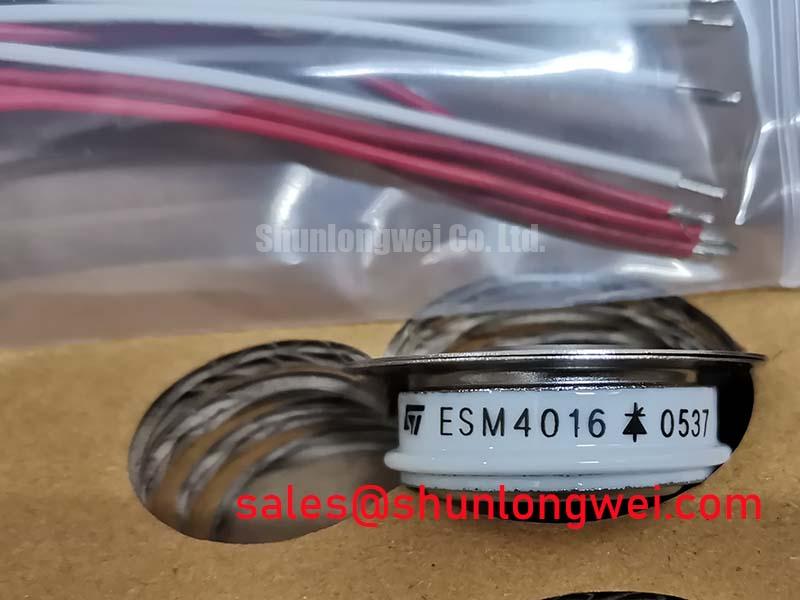
The ESM4016 from STMicroelectronics is an IGBT module rated at VCES = 1200 V as an Official Datasheet Specification. Its listed package is ISOTOP. The supplied data identifies current capability as Standard Operating Current; the system integrator should obtain the original manufacturer documentation before assigning a continuous or pulsed current limit. This distinction matters during repair assessment because the inverter bus voltage, cooling assembly, switching waveform, and protection threshold determine whether the installed duty remains appropriate.
| Parameter | Value | Status |
|---|---|---|
| Product model | ESM4016 | Official identification |
| Manufacturer | STMicroelectronics | Official identification |
| Collector emitter voltage | 1200 V | Official Datasheet Specification |
| Current rating | Standard Operating Current | Official supplied product data |
| Package | ISOTOP | Official Datasheet Specification |
For a pulsed-load investigation, begin by recording the heatsink temperature, DC link voltage, switching frequency, pulse duration, and measured collector current at the moment protection operates. A thermal model must not treat the semiconductor junction and heatsink as a single instantaneously equal temperature. During short high-energy pulses, junction temperature rises according to the transient junction to case thermal impedance, while the case and heatsink respond later. Engineers should use the transient thermal impedance curve and the relevant loss waveform from the original documentation to calculate a peak junction estimate.
This is an Engineering Calculation, not an ESM4016 factory temperature claim. Switching loss, conduction loss, case interface condition, repetition rate, and cooling path all contribute. A measured case temperature that appears moderate can therefore coexist with excessive junction excursion during repetitive overload events. In an industrial inverter welder or medium-frequency induction heating supply, capture the current waveform and collector emitter waveform together. A distorted pulse, extended current interval, or abnormal voltage excursion can change the loss estimate materially.
Inspect the ISOTOP mounting surface for flat contact, contamination, and uneven clamp loading. Design Consideration: minimize thermal interface resistance with a clean, controlled mounting process, then confirm the actual thermal response under the installed duty cycle rather than inferring it from an unloaded bench test.
Bench Tip: Keep gate and power terminals discharged and use ESD controlled handling while recording cold-state readings, because a comparison against the same equipment topology is more useful than an isolated meter result.
ESM4016 Circuit Protection & Reliability: Calibrating Static and Dynamic Current Distribution
Where multiple switching positions share current, static balance and switching balance require separate checks. IGBT conduction behavior can exhibit a positive temperature coefficient over relevant operating conditions, which can assist steady-state current sharing, but it does not guarantee equal dynamic sharing. Gate loop resistance, trace length, source or emitter return arrangement, drive timing, and local stray inductance can shift turn-on and turn-off current between parallel paths.
Design Consideration: route each gate drive return with its corresponding power return as symmetrically as the assembly permits, and validate the result with time-aligned waveform measurements. Unequal gate-loop inductance can alter Miller plateau behavior and cause one position to switch earlier or later than another. The resulting current imbalance may appear only during a specific load transition, so DC resistance checks alone are insufficient.
For protection investigation, confirm that the controller senses the correct current path and that any desaturation or overcurrent response is evaluated against real switching conditions. Do not assign a failure cause from one waveform snapshot. Compare gate emitter voltage, collector emitter voltage, current, and DC link behavior across repeated controlled tests. When insulation stress or unexplained leakage is suspected, technicians can review the principles of Partial Discharge Detection in High Voltage Power Modules; such testing requires suitable high-voltage procedures and does not establish an ESM4016 specific qualification.
For alternative device evaluation, K420A4001 should be assessed only against the original circuit requirements, including voltage rating, current conditions, package geometry, terminal arrangement, drive behavior, cooling interface, and protection calibration.
ESM4016 Thermal Electrical Optimization: DC Link Capacitance Bank Layout and Low ES Practical Tuning
The DC link capacitor bank should be evaluated as part of the switching loop, not as a remote energy reservoir. During turn-off, peak collector emitter voltage is influenced by DC link voltage plus the product of loop inductance and current-change rate. This Engineering Calculation establishes why a compact commutation path, close capacitor placement, and low-inductance bus geometry are important, but the permitted inductance and switching rate must be determined from measured peak voltage margins in the actual system.
In a repair build, inspect capacitor connections, laminated busbar contact faces, fastener tightness, and the physical path from capacitor terminals to the ESM4016. Long return paths and loosely arranged conductors can increase overshoot and ringing. A film snubber, when used by the original topology, should remain physically close to the switching loop so that its intended high-frequency function is not weakened by interconnect inductance. Engineers should verify waveform behavior at the module terminals with an appropriate high-bandwidth measurement setup.
Low-loss practical tuning should start with the existing gate drive and protection arrangement. Adjustments to gate damping or active clamping are Engineering Recommendations only after observing ringing, switching loss, peak voltage, and thermal response. For broader context when evaluating modern SiC or GaN substitutions at the system level, see Wide Bandgap Revolution. A faster switching technology can alter protection, layout, and EMI behavior and should not be treated as a drop-in conclusion.
ESM4016 Operational Boundaries: Evaluating Overvoltage Trip Prevention and Switching Limits
In converter equipment with regenerative energy, an overvoltage event may be associated with the DC link absorbing energy faster than the normal load can consume it. For systems that use a braking switch and ballast resistor, the energy path, trip threshold, resistor thermal capability, duty cycle, and controller timing must be checked as a system. The ESM4016 has an Official Datasheet Specification of 1200 V collector emitter rating, but this does not define the equipment operating threshold, transient allowance, or braking circuit settings.
When an inverter welder or induction heating power supply trips during rapid load change, first determine whether the DC link actually rises, whether the gate command is removed as intended, and whether the protection event precedes or follows the voltage disturbance. Inspect the braking path, capacitor connections, current sensing path, and control signals under controlled conditions. A trip can originate from several interacting conditions, including load behavior, drive sequencing, measurement reference error, or switching-loop overshoot.
Design Consideration: preserve creepage and clearance appropriate to the complete assembly voltage and contamination environment, and verify them against applicable equipment requirements. The ESM4016 package and 1200 V rating provide key selection facts, while the final electrical, thermal, and protection boundaries remain system-determined and should be confirmed through measured operating tests.