



Content last revised on September 25, 2026
STPS12045TV Circuit Protection and Reliability Under Industrial Conditions
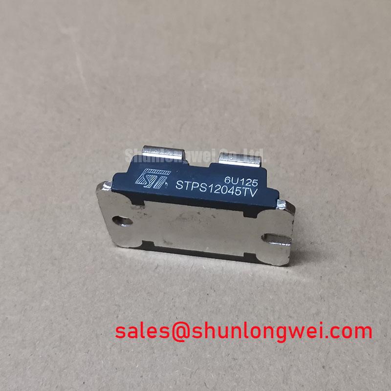
For a repair engineer, the first reliability task is to compare the failed circuit position with the actual electrical role of the component. The product is identified as STPS12045TV from STMicroelectronics, a power Schottky rectifier with a nominal 12 A current rating, a 45 V repetitive peak reverse-voltage rating, and a TO-220AB package. A position in a welder input rectifier, freewheel path, auxiliary supply, or induction heating converter may expose a semiconductor to very different current waveforms. The 12 A rating alone does not establish permissible surge current, repetitive peak current, junction temperature, or switching frequency. These values must be interpreted using the applicable STMicroelectronics documentation and the original equipment design record.
This distinction matters during equipment repair. The requested application brief refers to IGBT gate control, active Miller clamping, negative gate bias, braking choppers, and high-speed switching. STPS12045TV is a rectifier diode, not a gate-controlled IGBT module, so those functions must not be attributed to this part. A system integrator evaluating the device for an industrial inverter welder or medium-frequency induction-heating power supply should first establish whether the installed circuit requires a rectifying diode, an IGBT switching module, or another power-semiconductor function.
| Parameter | Product data | Engineering interpretation |
|---|---|---|
| Manufacturer | STMicroelectronics | Confirm the marking and procurement documentation against the installed assembly |
| Part number | STPS12045TV | Use the complete suffix during documentation and replacement review |
| Device type | Power Schottky rectifier | Evaluate it as a diode rather than as a gate-controlled switching module |
| Current rating | 12 A nominal rating | Interpret the rating using the specified temperature, mounting, waveform, and cooling conditions |
| Reverse-voltage rating | 45 V | Do not treat this rating as a recommended continuous DC-bus voltage; include transients and operating margin in the system design |
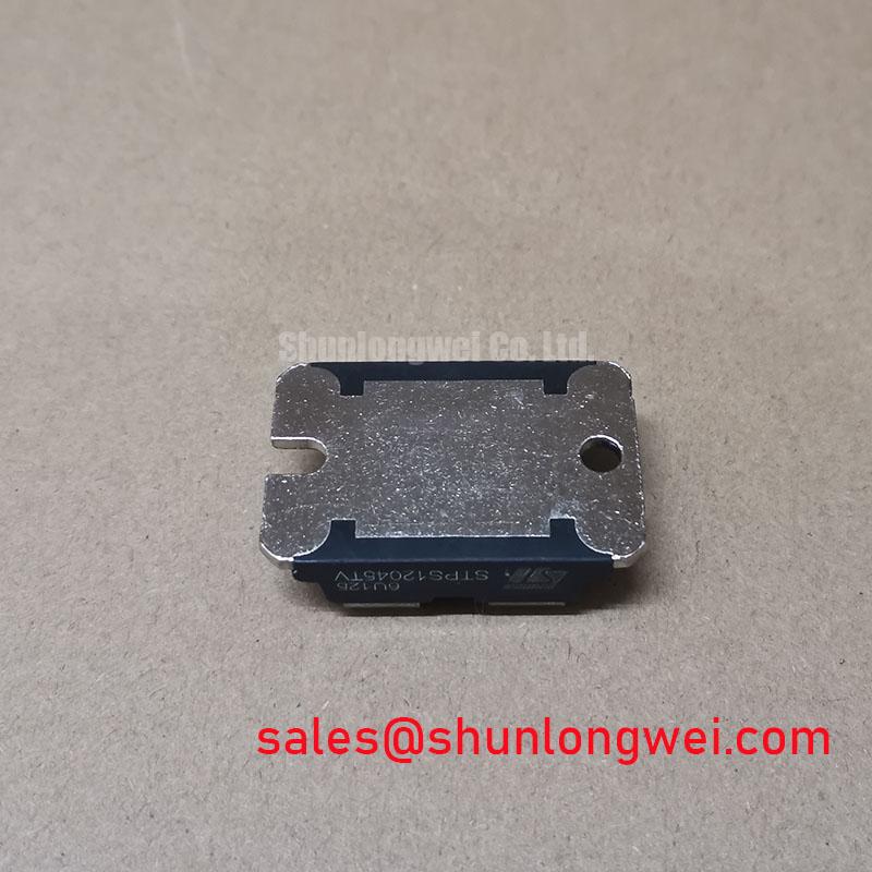
| Package | TO-220AB | Confirm polarity, lead arrangement, mounting, tab isolation, and thermal-interface details from the applicable datasheet |
STPS12045TV Circuit Protection and Reliability Under Industrial Conditions
For a repair engineer, the first reliability task is to compare the failed circuit position with the actual electrical role of the component. A position in a welder input rectifier, freewheel path, auxiliary supply, or induction-heating converter may expose a semiconductor to very different current waveforms. The 12 A rating alone does not establish permissible surge current, repetitive peak current, junction temperature, or switching frequency. These values must come from the applicable STMicroelectronics documentation or from the original equipment design record.
Atmospheric neutron radiation and altitude-related reliability are legitimate subjects for high-reliability power conversion, but a specific FIT value or Single Event Burnout rate cannot be calculated from the supplied information. Such an assessment would require a qualified radiation model, device technology data, mission profile, voltage-stress distribution, altitude-exposure data, and an authoritative reliability source. A repair page should therefore avoid assigning a neutron-induced failure probability to this component or claiming a guaranteed altitude derating factor.
At elevations above the equipment manufacturer’s tested operating range, designers should review cooling performance, insulation coordination, creepage, clearance, and the actual electrical stress across the rectifier. Reduced air density can affect external insulation and convection, while the semiconductor junction remains governed by its own thermal path and operating conditions. The final limits should be taken from the equipment qualification file and the component manufacturer’s published ratings, rather than from a generic altitude rule.
During a field inspection, compare the suspected rectifier with a known-good signal path where available. Look for cracked encapsulation, discolored terminals, loose busbar joints, degraded insulation, and signs of localized heating. With the equipment isolated and discharged, measure for unexpected low impedance between the relevant power terminals. A resistance reading by itself is not a complete semiconductor health test because parallel capacitors, snubbers, transformers, and other semiconductor paths can influence the result.
For an inverter welder or medium-frequency induction-heating supply, record the DC-link voltage, current waveform, ambient temperature, heatsink condition, and operating state before replacing the device. Verify that the circuit position is a rectifier or freewheel position compatible with a Schottky diode. STPS12045TV does not provide the gate terminal, Kelvin-emitter connection, active Miller-clamp compatibility, or negative off-state bias associated with an IGBT gate-controlled module.
Technical background on switched converter structures can be reviewed through Switched-Mode Power Supply topologies and conversion. Semiconductor carrier behavior is discussed in Drift Velocity and Carrier Mobility in Silicon and WBG Semiconductors, but neither reference replaces the specific STMicroelectronics rating data required for a production decision.
Field Diagnostics and Commissioning for Terminal and Impedance Verification
Commissioning should begin with a drawing-level comparison. Confirm the terminal names, polarity, parallel connections, and the position of any RC network or clamp before removing the original device. STPS12045TV uses a TO-220AB package, but the system integrator should still verify the required lead arrangement and polarity from the applicable datasheet and equipment documentation rather than transferring wires by physical position alone.
In long-cable welding and induction-heating systems, parasitic inductance and impedance mismatch can produce overshoot at semiconductor terminals. A reflected waveform may increase stress, but the magnitude cannot be stated as a fixed multiple without cable construction, termination, busbar geometry, switching speed, and measurement bandwidth. Engineers should observe the relevant terminals with a properly rated differential probe and compare the result with the equipment DC link and the rectifier’s 45 V reverse-voltage rating.
Output filters, chokes, and damping networks should be selected from the measured current spectrum, cable arrangement, control response, and allowable voltage ripple. Their values are system-determined. The practical objective is to limit ringing and overshoot while avoiding excessive loss, resonance, or control-loop interaction. A filter added without checking the complete power path can move the stress to another component or create an unstable operating condition.
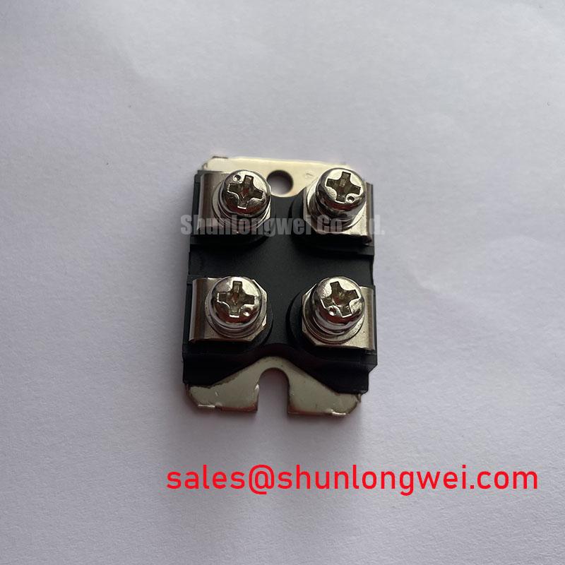
Terminal verification also includes mechanical inspection. Busbars should sit flat against the intended mounting surfaces, fasteners should be tightened according to the equipment or component manufacturer’s instructions, and unsupported conductors should not transfer vibration into the terminals. Thermal compound, insulating sheets, and washers should be checked for correct placement where the assembly uses them. Do not assume that the TO-220AB tab is electrically isolated from the internal semiconductor connection unless the original documentation explicitly confirms it.
Bench Diagnostic: Disconnect power and verify the DC link has reached a safe state before inserting, removing, or probing any power semiconductor or cable.
Where an alternative device is being evaluated, the comparison must include electrical function, terminal topology, voltage and current ratings, transient capability, thermal resistance, mounting geometry, and qualification status. The SKM75GB07E3 is a separate power-semiconductor product and should be reviewed as an independent device, not treated as a direct substitute for STPS12045TV without a complete engineering comparison.
Benchtop Waveform Tuning and Overvoltage Trip Prevention
A benchtop waveform test should reproduce the actual operating topology with controlled voltage, current, load, and protection settings. The purpose is to identify terminal overshoot, ringing, recovery behavior, commutation interaction, and thermal rise before the equipment returns to service. STPS12045TV is a Schottky rectifier, so it should not be assigned the role of an internal braking IGBT or high-power ballast switch. Its switching and recovery behavior must be evaluated in the confirmed rectifier position using the applicable datasheet information and measured circuit waveforms.
In a converter that uses a separate braking transistor, the braking device and resistor are selected from the motor or load deceleration profile, DC-link behavior, pulse duration, duty cycle, thermal path, and fault response. The resistor must be evaluated for pulse energy as well as average power. The braking transistor must be evaluated for its voltage stress, current waveform, switching loss, short-circuit response, and cooling. These are system calculations and cannot be derived from the 12 A rectifier rating alone.
For a power-semiconductor position associated with rectification or freewheeling, observe the commutation interval and the interaction between the diode and its clamp network. A fast voltage transition can expose layout inductance, diode recovery effects, or an incorrectly placed snubber. Keep the measurement loop physically compact, use a probe connection suitable for fast transients, and verify that the displayed ringing is not created by the probing arrangement.
Overvoltage protection should be coordinated with the verified 45 V reverse-voltage rating, the normal DC-link range, fault-clearing time, and the energy available from the load. The trip threshold cannot be selected from the diode rating alone. The correct procedure is to measure the highest normal and abnormal voltage and validate the protection response under controlled tests while maintaining suitable margin below the component limits.
Gate-drive timing is not applicable to STPS12045TV because it is a rectifier diode. If the equipment also contains a separate gate-controlled transistor, inspect that circuit independently. Applying a gate pulse, negative bias, or active Miller clamp to STPS12045TV would be an invalid test and may damage the assembly. A circuit diagram and authoritative pin definition are necessary before any gate-drive experiment on another device.
STPS12045TV Thermal and Electrical Integration Review
Thermal evaluation should begin with the real current waveform rather than the nominal label current. The 12 A rating must be interpreted alongside conduction duration, commutation conditions, ambient temperature, heatsink performance, interface materials, airflow, and enclosure temperature. A precise heatsink size or continuous operating point cannot be stated without the manufacturer’s thermal parameters and the actual assembly conditions.
Designers should inspect the complete current loop and minimize parasitic inductance where it can create switching overshoot or unwanted ringing. Power and control conductors should be separated according to the equipment layout, and sensitive feedback wiring should not share a noisy return path with high di/dt current. If the assembly contains a gate-controlled semiconductor elsewhere in the topology, its gate loop should be treated as a dedicated circuit with short, well-controlled return routing. That recommendation does not establish that STPS12045TV itself has a gate or Kelvin-emitter connection.
Negative gate bias and active Miller clamping are specialized techniques for verified IGBT or MOSFET gate-drive circuits and are not functions of STPS12045TV. Engineers working on a separate IGBT stage may consult Evolution of Negative Off-Bias Gate Drive Circuits as an engineering reference, while keeping that guidance separate from this rectifier.
Dead time, pulse width, gate resistance, damping, and active-clamp timing are determined by the confirmed switching device, driver architecture, parasitic inductance, temperature, and measured waveform. The correct tuning method is to begin with the original equipment values, verify the driver output with the power stage disabled, and then progress through controlled low-energy tests. Oscilloscope measurements should check both the commanded signal and the actual semiconductor terminal response.
For procurement and repair records, retain the complete STPS12045TV designation, the stated STMicroelectronics manufacturer identity, the 12 A current information, the 45 V reverse-voltage rating, the TO-220AB package description, and the verified equipment position. Before approving installation, confirm the polarity, thermal data, mounting requirements, and applicable transient or surge ratings from the correct technical documentation. This documentation-based process prevents an unverified IGBT-control assumption from being carried into an industrial inverter welder or medium-frequency induction-heating repair.