



Content last revised on September 29, 2026
Assembly Integrity and Layout Architecture for Thermal Cycling Margins
| Specification | Official Value |
|---|---|
| Manufacturer | Infineon |
| Product category | IGBT Module |
| Package | Module |
| Rated voltage | 1200 V |
| Rated current | 100 A |
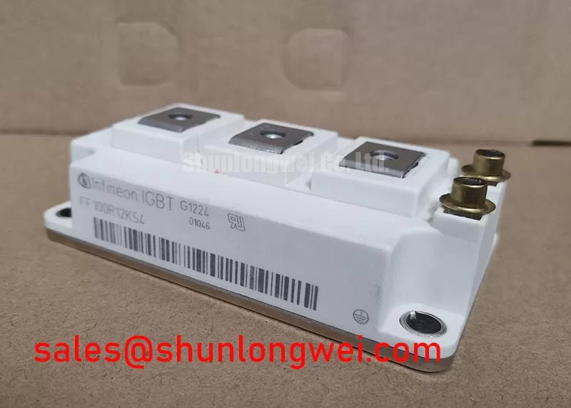
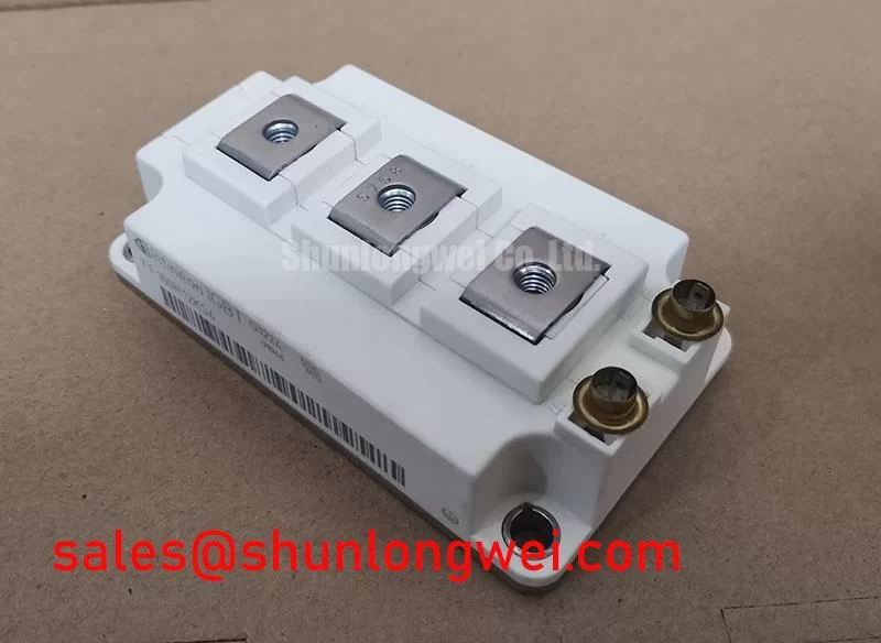
Inspect the braking branch, DC link connections, mounting surface, and ballast-resistor wiring for discoloration, looseness, contamination, or abnormal contact resistance before energizing the inverter. The FF100R12KS4 is an Infineon IGBT Module with an official rated voltage of 1200 V and rated current of 100 A; these values define the product identity, while the allowable switching, overload, thermal, and short-circuit conditions must be checked against the original technical documentation and the complete converter design.
For an industrial inverter welder or medium-frequency induction-heating supply, the internal or external braking path must be evaluated as a system. The braking IGBT and high-power ballast resistor are exposed to deceleration energy, DC-link transients, and repeated thermal cycling. Confirm that the resistor network, fuse coordination, bus capacitors, current sensors, and controller timing are compatible with the replacement module. The module rating alone does not establish the permissible braking energy or repetition rate.
Keep the high-current commutation loop compact and physically separated from gate-drive and sensing conductors. Minimize stray inductance in the collector-emitter power path to reduce turn-off overshoot, then verify the resulting peak voltage with a properly rated differential probe during controlled switching tests. Clearance and creepage should be determined from the working voltage, pollution environment, insulation system, enclosure, and applicable equipment standard rather than copied from a generic module installation.
When checking an installed unit, compare the gate-emitter waveform with a known-good phase position and inspect the collector-emitter waveform at the module terminals. Unequal switching edges may indicate gate-loop impedance variation, an unstable driver supply, poor emitter reference, or an assembly problem. The diagnostic path should include the gate resistor, driver return, isolation interface, clamp network, and local decoupling, because a power-device replacement does not remove faults elsewhere in the switching cell.
For comparative procurement, FZ1800R12KF4_S1 can be reviewed as a separate Infineon module option, but its electrical compatibility, mechanical footprint, gate-drive requirements, and thermal interface must be assessed independently. A similar voltage class does not by itself prove drop-in interchangeability.
Maintenance Note: Monitor contact temperature during scheduled inspections and keep the heatsink, fan path, and surrounding air channels free of dust and moisture condensation.
Operational Boundaries and High-Frequency Common-Mode Current Evaluation
Probe the motor phase terminals and DC link at the module-side connection first when a drive shows excessive bearing current, cable-end ringing, or unexplained insulation stress. Long motor leads can behave as transmission lines, and impedance mismatch may create reflected-wave peaks that approach twice the local DC-link voltage under particular installation conditions; the actual result depends on cable construction, length, termination, switching edge, motor impedance, and measurement position.
This is a Design Consideration, not an official FF100R12KS4 limit. Evaluate the complete output path, including phase conductors, motor cable shield, motor-frame bonding, common-mode choke, dv/dt filter, and bearing-current mitigation. Filter selection should be based on measured edge behavior, motor insulation requirements, allowable leakage current, thermal loss, and the control loop response. The converter designer should verify peak voltage margins against the DC-link voltage during switching tests.
In a phase-controlled front end, conduction angle affects DC-link ripple, input current distortion, and the operating burden placed on the downstream switching stage. Check the line-frequency ripple at the bus under the intended load range and review the rectifier control sequence against the inverter gate timing. Harmonic reduction cannot be inferred from the IGBT module rating; it depends on the rectifier topology, control algorithm, line impedance, passive filtering, and compliance target for the finished equipment.
An RC snubber or clamp network may reduce local transient energy when its impedance and damping are matched to the actual commutation loop. Treat the component values as system-dependent engineering variables. Validate them with current and voltage probes at the module terminals, then inspect whether the network introduces excessive switching loss, resistor heating, or unwanted interaction with the gate driver.
For a front-end or auxiliary power stage used alongside the inverter section, engineers may also evaluate FZ2400R17KF4 as a separate device in the power topology. It should be considered on its own voltage, current, package, switching, isolation, and thermal requirements rather than treated as an automatic companion to the FF100R12KS4.
The official Infineon portfolio provides the appropriate manufacturer-level context for IGBT families and application categories; consult the Infineon IGBT Modules and Discretes Official Portfolio when correlating product-family documentation with the actual converter design.
Field Diagnostics and Commissioning of Thermal Transients
Record the case temperature, heatsink temperature, load current, switching frequency, and duty pattern during the same pulsed-load event before interpreting a thermal alarm. A single temperature reading cannot describe the junction condition of the FF100R12KS4, because junction temperature follows the power pulse and the thermal path from semiconductor junction to case, interface material, heatsink, and ambient air.
Use the measured electrical waveform to estimate instantaneous conduction and switching losses, then apply the manufacturer’s thermal impedance data and the converter’s real pulse sequence. A multi-RC thermal model can represent short and long thermal time constants, but the model parameters must come from the applicable technical documentation or validated laboratory measurements. The peak junction estimate should be compared with the documented operating boundary and the actual recovery time between pulses.
When a unit trips after repeated welding pulses or induction-heating bursts, inspect the thermal interface for pump-out, uneven compression, contamination, or local dry areas. Check whether the heatsink surface is flat and whether airflow is reaching the module rather than recirculating around the enclosure. Thermal behavior may also be influenced by gate-drive timing, current sharing, bus ripple, snubber loss, and sensor placement, so avoid assigning the trip to junction temperature without correlating the electrical and thermal records.
Commissioning should begin with reduced energy and a controlled duty pattern, followed by oscilloscope verification of gate-emitter voltage, collector-emitter voltage, phase current, and DC-link behavior. Increase operating stress only after the measured waveforms remain consistent across the relevant load range. Designers should verify the full transient thermal response under the intended overload profile, since the official 1200 V and 100 A ratings do not replace application-specific switching and thermal limits.
For installations exposed to high humidity or repeated temperature changes, check for condensation traces around the module, busbar insulation, driver board, and sensor connectors during preventive maintenance. Moisture control, enclosure heating, airflow, and insulation monitoring are equipment-level design considerations. The module should not be assigned an environmental certification or lifetime expectation that is not documented for the complete assembly.
Thermal interface practice and cooling architecture can be compared with the maintenance principles discussed in The Advanced Thermal Management Revolution. The article is a technical reference for thermal-management evaluation, not a substitute for the FF100R12KS4 manufacturer documentation.
Benchtop Waveform Tuning and Desaturation Protection
Capture the gate command, gate-emitter voltage, collector-emitter voltage, and collector current on the same time base when testing desaturation protection or a suspected short-circuit event. The measurement should show whether the driver detects abnormal collector-emitter behavior quickly enough, whether the protection threshold is stable, and whether the turn-off action creates an excessive inductive voltage transient.
Short-circuit withstand time, desaturation response, soft turn-off behavior, and safe operating limits are manufacturer-specific characteristics. They must not be inferred from the 1200 V voltage rating or 100 A current rating alone. Confirm the applicable short-circuit information, gate-drive conditions, test circuit, and temperature range in the original Infineon documentation before setting protection timing.
A two-stage soft turn-off sequence can be evaluated as an Engineering Recommendation when the gate driver supports it: first reduce the current transition rate, then complete turn-off under controlled conditions. The required timing, gate resistance, clamp behavior, and negative or zero gate bias are system-determined. Tune them against measured collector-emitter overshoot, driver isolation performance, parasitic inductance, and the protection response of the finished converter.
During bench testing, keep the probe ground arrangement appropriate for the switching node and use measurement equipment rated for the expected common-mode voltage. Compare the protected event with a low-energy commissioning pulse, then inspect the gate driver supply, desaturation diode path, blanking behavior, fault latch, and reset sequence. A missing fault signal may result from the sensing network, isolation channel, controller logic, or probe configuration rather than the power module itself.
After a protection event, record the waveform and inspect the module, busbar joints, gate terminals, driver board, and snubber components before repeating the test. Verify that the control system cannot immediately reapply gate drive while the cause remains unresolved. The final protection behavior should be validated under the intended DC-link condition, load topology, cable arrangement, and thermal state by the equipment design team.