


Content last revised on September 29, 2026
Benchtop Waveform Tuning: Baseplate Thermal Interface Control on FF300R12KE3
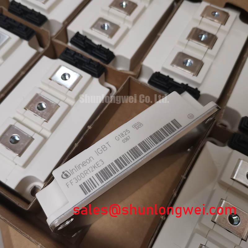
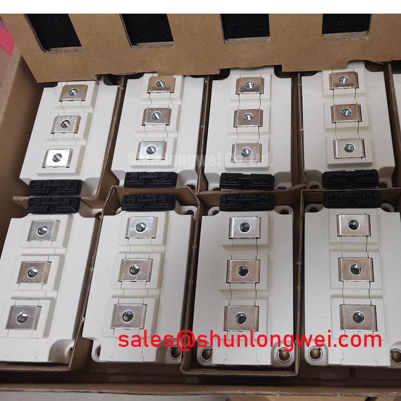
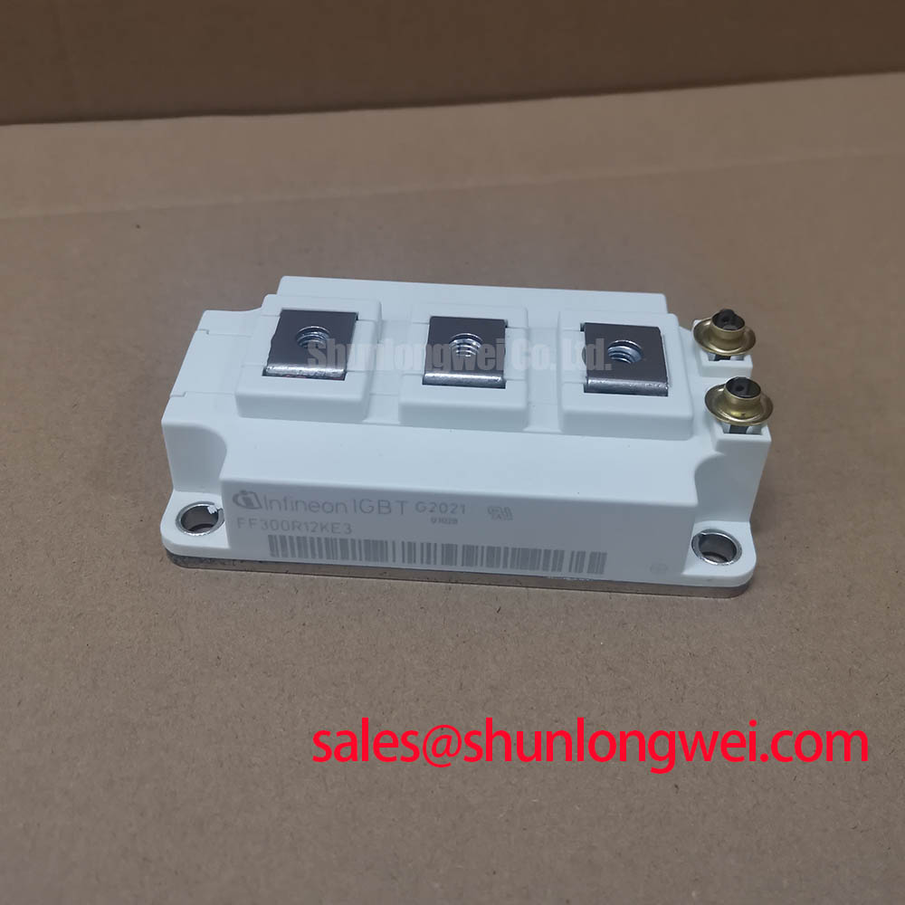
FF300R12KE3 | Infineon | IGBT module | Rated blocking voltage: 1200 V (Official Specification) | Rated current: 300 A (Official Specification) | Package: module (Official Specification)
Measure collector-to-emitter and gate-to-emitter resistance with the drive isolated and the DC link confirmed discharged, then compare both results with a known-good phase position. A short indication warrants investigation; a single cold multimeter reading cannot establish switching health. Record terminal positions and lead routing before removal so the replacement can be checked against the original installation rather than against assumptions about other IGBT modules.
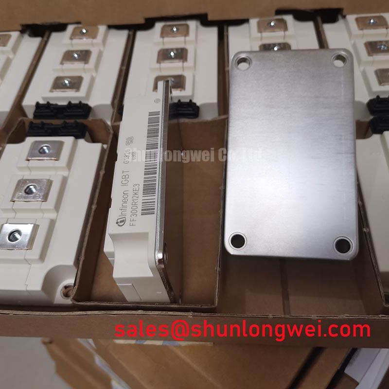
Inspect the mounting surface for debris, old thermal compound, raised edges and uneven contact marks. As a Design Consideration, apply thermal interface material as a continuous thin layer that fills surface irregularities without creating a thick insulating gap. Check the baseplate and heatsink contact pattern rather than prescribing a grease thickness: surface condition, compound properties and the equipment’s mounting instructions determine the finished interface. Seat the module evenly and tighten its fasteners in a progressive sequence using the applicable hardware and mounting guidance.
Field alert: Do not tighten one mounting fastener fully while the opposite side of the baseplate remains unseated.
Once mechanical contact is established, capture turn-on and turn-off waveforms under a controlled test condition. Compare collector-to-emitter overshoot, gate voltage and heatsink temperature with the corresponding phase position. A temperature difference may indicate an interface or airflow problem, while an abnormal switching trace may point to the gate circuit or bus layout; neither observation proves a single cause. For context on how thermal paths affect power-module integration, see The Advanced Thermal Management Revolution.
FF300R12KE3 Circuit Protection and Reliability: Checking Gate Drive Isolation
Probe the gate voltage relative to its local emitter reference during a controlled switching test, and look for unintended pulses when the opposing switch changes state. If pulses appear, inspect the driver supply, isolation arrangement, gate return and coupling across the power-stage layout. The 1200 V module rating is an Official Specification; it is not a specification for the external driver’s isolation barrier or common-mode transient immunity. Select and verify those driver properties against the equipment’s insulation requirements and measured switching conditions.
Trace the installed protection path from the DC link to the switching terminals. Check whether an RC snubber is present, where it connects and whether its components show damage or changed measurements. As a Design Consideration, a suitably designed snubber can reduce switching transients, but its values belong to the original circuit design and must be assessed against measured waveforms. A motor drive’s input rectification, DC-link ripple and inverter switching are separate functions: line-frequency ripple on the bus should not be mistaken for a phase-angle command at this IGBT’s gate.
If the drive uses a bootstrap-supplied high-side driver, examine its supply waveform through the actual operating sequence. Charge availability, discharge during switching and the bootstrap diode’s recovery behaviour are driver-circuit questions, not published FF300R12KE3 ratings. Likewise, inspect any installed MOV network in relation to the bus protection scheme; an MOV does not replace verification of turn-off overshoot at the module terminals. The Infineon IGBT portfolio and Infineon IGBT modules overview provide manufacturer context, while the equipment schematic determines which protections apply to this assembly.
Assembly Integrity and Layout Architecture: Checking Dynamic Gate Impedance on FF300R12KE3
Capture gate-to-emitter voltage at the module connection while the adjacent switch commutates, then compare the trace with the driver output. A difference between those locations can expose voltage developed along the gate loop. Keep the gate and return paths short and closely coupled as a Design Consideration to limit induced disturbance; confirm the result by measuring the installed circuit rather than assigning a universal layout limit.
Where the existing driver includes an active Miller clamp, verify its connection and operating sequence. Where it uses negative off-state bias or separate turn-on and turn-off impedances, assess those features against the original driver design. None is an inherent FF300R12KE3 specification, and no bias or resistor value should be transferred from another drive without checking its gate waveform and device limits. Inspect terminal tightness and the gate connector at the same time: a poor connection can make a correctly configured driver appear inconsistent under switching.
For a heavy-duty variable-frequency AC motor drive under compatibility review, match the replacement against the equipment’s topology, terminal arrangement, mechanical fit, cooling interface and driver settings, as well as its voltage and current requirements. The 300 A rating (Official Specification) alone does not establish interchangeability. FZ1800R12KF4_S1 is a separate Infineon part to compare at the specification and drawing level, not a drop-in substitute inferred from its name. In a wider converter schematic, FS100R12KT4G_B11 is likewise a distinct module whose possible role depends on the actual power-stage design.
FF300R12KE3 Thermal-Electrical Optimization: Investigating Motor-Terminal Voltage Spikes
Measure the switching waveform at the module output and, where the installation permits, at the motor terminals using probes and procedures appropriate to the drive. A spike concentrated at the motor end of a long cable may involve reflected-wave behaviour; a spike at the module terminals calls for a closer look at the DC-link loop and switching layout. Do not treat motor-terminal voltage and collector-to-emitter voltage as the same measurement, or assume a fixed voltage-doubling result for every cable and motor.
Check cable length, routing, termination and the presence of an output filter against the equipment drawings. As a Design Consideration, a drive-output filter or choke may be evaluated when measured motor-terminal stress and cable conditions warrant it. Filter selection is a system decision involving switching behaviour, motor insulation, operating current and thermal performance. Repeat waveform measurements after any approved change so that improvement at the motor does not conceal added heating elsewhere.
During the same run, log heatsink temperature and compare phase currents under equivalent operating conditions. Unequal heating may reflect mounting contact, airflow or electrical imbalance; resolve those possibilities with measurements rather than attributing it to current sharing inside the module. If the protection log records a surge event, inspect the relevant upstream and power-stage paths before restart. The 300 A rated current does not state a permissible surge-current limit or a safe recovery interval after a junction-temperature excursion; those decisions require the applicable device data and the drive’s protection records.