

Content last revised on September 22, 2026
Assembly Integrity & Layout Architecture: Implementing Galvanic Gate Drive Isolation, Reinforced for FP25R12W2T4_B11
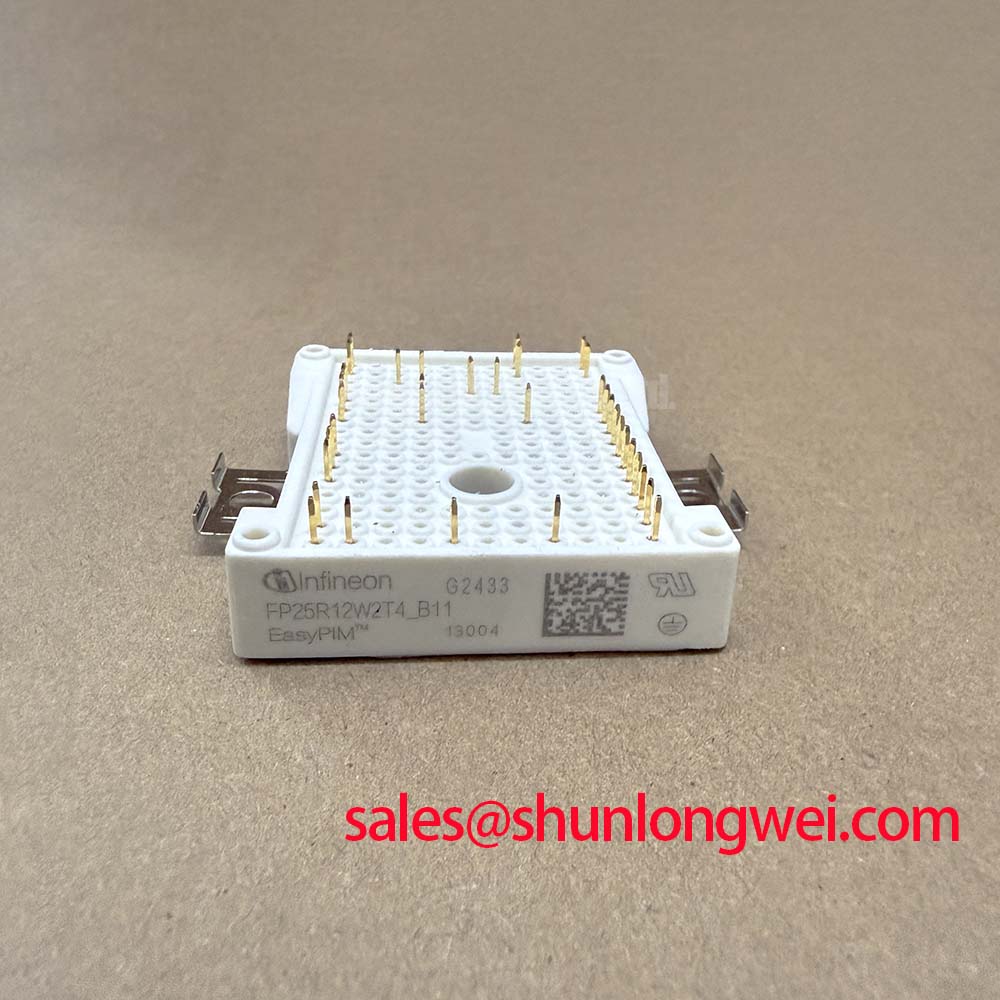
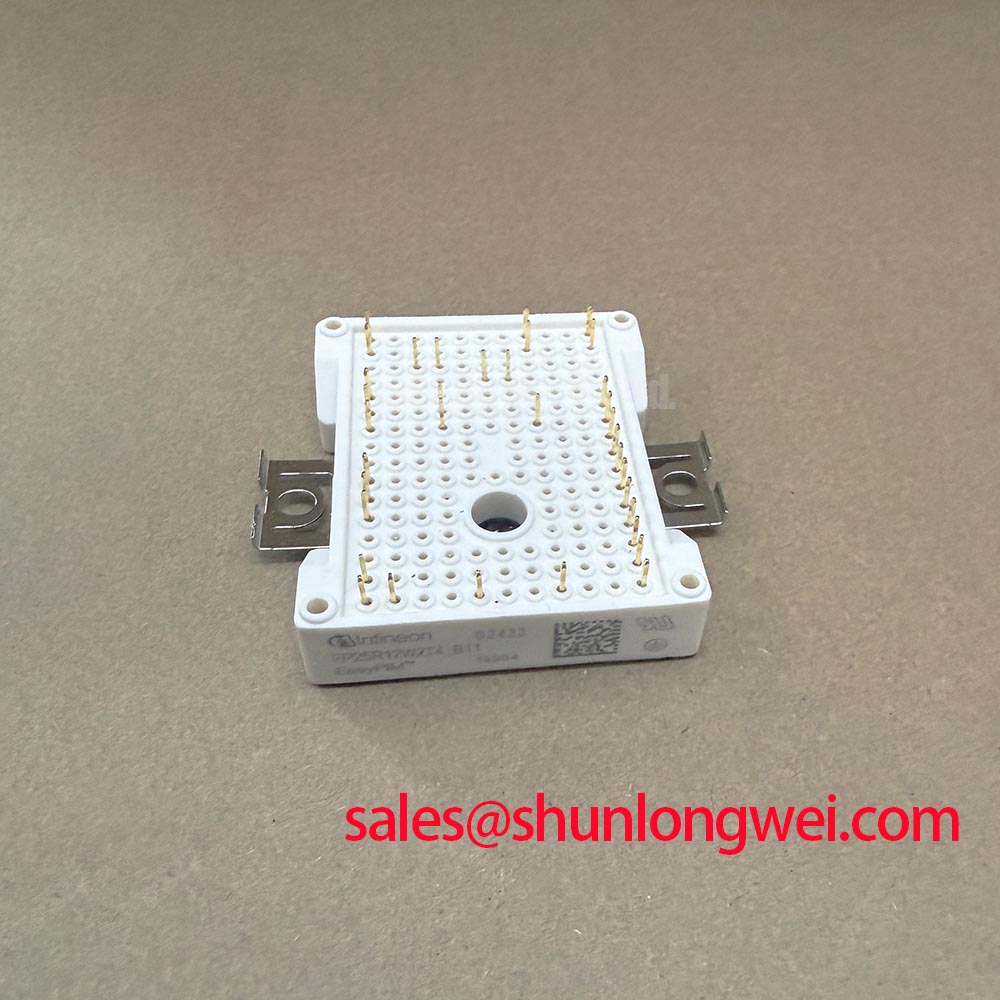
Before installation, verify the nameplate and compare the removed drive module’s electrical boundary with the replacement: FP25R12W2T4_B11 is an Infineon IGBT module rated at VCES = 1200 V and IC nom = 25 A under its official datasheet conditions. Its official maximum junction temperature is 150 °C, total power dissipation is 195 W at TC = 25 °C, and junction-to-case thermal resistance is 0.64 K/W per IGBT. These ratings identify the module’s electrical and thermal limits; they do not independently confirm compatibility with a particular inverter control board, gate driver, heatsink, or protection circuit.
| Official specification | Value |
|---|---|
| Manufacturer | Infineon |
| Collector-emitter voltage, VCES | 1200 V |
| Nominal DC collector current, IC nom | 25 A |
| Total power dissipation at TC = 25 °C | 195 W |
| Junction-to-case thermal resistance per IGBT, Rth(j-c) | 0.64 K/W |
| Maximum junction temperature, Tvj max | 150 °C |
Start the replacement assessment at the gate-driver interface rather than at the power terminals. With the inverter safely isolated and DC-link energy discharged according to the equipment procedure, inspect the driver board for contamination, cracked solder joints, loose connectors, damaged isolation barriers, and heat-darkened areas around gate resistors or desaturation protection circuits. A cold resistance check can identify a clear gate-to-emitter short or an abnormal low-resistance path, but it cannot validate switching behavior. The gate waveform and emitter reference must be checked under controlled operating conditions against the known-good channel or the original equipment documentation.
Galvanic isolation is a system-level requirement of the driver assembly, not an official electrical rating stated for this IGBT module. For high-dynamics CNC axes and robotics servo drives, the isolation barrier must tolerate the common-mode environment produced by the inverter. Where a drive design calls for reinforced isolation above 5 kV and common-mode transient immunity above 100 kV/μs, those values must be verified against the actual gate-driver, isolator, PCB spacing, and system safety documentation. They should not be treated as intrinsic specifications of the FP25R12W2T4_B11.
Design Consideration: keep the gate-drive loop compact, ensure the gate-return path follows the intended emitter reference, and separate sensitive control traces from switching-node copper where the original board layout permits. A long or shared return path can convert load-current transients into apparent gate-voltage movement. This may contribute to irregular turn-on behavior, intermittent protection trips, or channel-to-channel waveform differences. Oscilloscope measurements should use a probing method suitable for fast switching signals and should compare the gate-to-emitter voltage with the collector-emitter waveform during controlled testing.
Clearance and creepage distances are determined by the assembled drive, working voltage, pollution degree, material group, and applicable equipment standard. Do not alter isolation slots, protective coatings, or spacing around the gate-driver barrier simply to accommodate a repair. If repeated driver-board faults occur after module replacement, investigate DC-link ripple, grounding paths, cooling airflow, and control-board supply stability before attributing the issue to the IGBT module itself.
For substitution assessment, terminal arrangement, driver interface, protection strategy, thermal interface, and inverter topology require independent verification. The FP10R12KE3 can be reviewed as a related Infineon 1200 V module reference, but its current capability and physical integration must be compared with the original equipment requirements before any replacement decision.
Benchtop Waveform Tuning: Mitigating Stress via Baseplate Convexity Compensation and Screw on FP25R12W2T4_B11
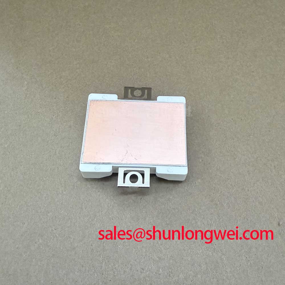
Inspect the heatsink contact face before fitting the module. Remove old thermal compound without scratching the mounting surface, then check for embedded debris, corrosion, burrs, or uneven residue that could create local air gaps. The official 0.64 K/W junction-to-case thermal resistance per IGBT describes heat transfer from the semiconductor junction to the module case under defined conditions. The installed thermal path also depends on the condition of the baseplate contact, thermal interface material, heatsink flatness, mounting pressure, airflow, and ambient temperature.
Design Consideration: use a controlled, thin and uniform thermal interface layer rather than a heavy application that can trap voids. Thermal interface thickness in the range of 50 to 100 μm is a common integration reference where the material supplier, mounting system, and surface condition support it; it is not an Infineon specification for this module. Baseplate curvature and heatsink flatness should be evaluated together. A contact pattern that is incomplete after removal can indicate uneven pressure, an unsuitable interface material application, or a distorted mounting surface.
Tighten mounting screws in a balanced sequence that draws the module progressively onto the heatsink rather than fully loading one corner at a time. The correct screw size, washer arrangement, tightening method, and torque are determined by the module mechanical documentation and the equipment hardware. ⚠️ Maintenance Note: Periodically monitor heatsink contact temperature and verify that dust accumulation or restricted airflow has not raised the thermal load on the module.
Switching frequency affects total inverter heat because conduction and switching losses are both involved. A servo drive operating between 2 kHz and 16 kHz should therefore be assessed using its actual modulation method, current profile, DC-link voltage, cooling condition, and measured case temperature. The 195 W at TC = 25 °C value is an official dissipation rating at a controlled case temperature, not an assurance that the same dissipation can be removed in a closed cabinet at elevated ambient temperature. Engineers should confirm thermal margins using measured operating waveforms and the equipment’s approved thermal model.
Transient junction temperature is not represented by a single steady-state resistance alone. Where repair engineering requires a dynamic thermal estimate, Foster and Cauer network concepts can help interpret time-dependent heating behavior; see Foster and Cauer Thermal Network RC Models for Transient Junction Temperature. The final thermal decision must use the thermal impedance information and operating conditions applicable to the original drive.
Benchtop Waveform Tuning: Mitigating Stress via Calculating Failures in Time Rates in High-Altitude Installations for FP25R12W2T4_B11
No official FIT rate, terrestrial neutron susceptibility figure, altitude derating curve, or single-event burnout rate is provided in the stated factory parameters for the FP25R12W2T4_B11. A numerical reliability prediction would therefore be unsupported. It is not appropriate to assign a failure rate, operating-life estimate, or DC-bus derating percentage to this specific module without an applicable manufacturer qualification report, system mission profile, environmental model, and approved reliability methodology.
Design Consideration: installations above 2000 m can require a broader system review because air cooling and insulation coordination may differ from conditions at lower elevation. The required evaluation belongs to the complete drive assembly, including enclosure ventilation, DC-link architecture, gate-driver isolation, protective earth arrangement, and the system standard that governs the equipment. Verify the original machine documentation and applicable regional requirements before changing the permitted operating envelope.
For a drive removed from high-altitude service, record the practical evidence available at the equipment level. Check cabinet air paths, fan operation, inlet filter condition, condensation traces, moisture ingress, heatsink contamination, loose bus connections, and the consistency of case-temperature readings among phases. These checks do not determine a semiconductor FIT rate, but they can identify operating conditions that should be corrected before the repaired inverter returns to service.
Waveform review remains more useful than unsupported lifetime arithmetic. Under a controlled load, compare collector-emitter switching waveforms, gate-emitter behavior, DC-link ripple, and protection-event records with the machine’s healthy operating channel or validated reference data. A ringing change may indicate a layout, connection, driver, snubber, or measurement issue. It should be investigated as a system interaction rather than treated as proof of one isolated root cause.
The relationship between reverse-current behavior and inverter operation should also be understood from an appropriate technical source when the power stage uses reverse-conducting structures or comparable current paths. Infineon’s RCDC Reverse Conducting IGBT application note provides relevant device-level context. Its principles should be applied only after confirming that they match the exact module topology and original circuit design.
FP25R12W2T4_B11 Operational Boundaries: Evaluating Planar Symmetrical Busbar Geometry and Achievable Limits
Confirm the DC-link and phase-bus connections for mechanical security, correct phase routing, and equal contact quality before energizing the inverter. The module’s official 1200 V VCES rating establishes the collector-emitter blocking-voltage boundary, yet the voltage observed during switching can exceed the nominal DC-link voltage because parasitic inductance interacts with changing current. In engineering terms, the switching peak rises with the DC-link voltage plus the inductive contribution associated with loop inductance and current slew rate. The actual peak must be measured in the assembled inverter and evaluated against the applicable device limits.
Design Consideration: minimize the area of the high-current commutation loop so that stray inductance is reduced and turn-off overshoot is easier to control. Symmetrical planar busbar geometry can support this goal when it is compatible with the original drive’s clearances, terminal arrangement, insulation system, and service access. A numerical inductance target cannot be assigned from the provided product data. System engineers should verify peak voltage margin, ringing frequency, and current sharing through switching tests using the actual busbar, capacitor placement, cable length, and load condition.
DC-link capacitors and snubber components must be selected as elements of the inverter system, not as accessories defined by this module alone. Their required capacitance, ESR, ripple capability, placement, and thermal performance depend on the switching waveform and protection philosophy. Do not substitute a snubber value based only on another machine or module family. If the original suppression network has changed, inspect the resulting voltage waveform before committing the drive to continuous production duty.
Fast semiconductor fuse coordination also requires system-specific evidence. The module’s supplied specifications do not state a permissible fuse I2t value, surge-current limit, short-circuit withstand time, or safe operating duration during a fault. The fuse data, inverter protection timing, DC-link energy, contactor behavior, and controller response must be reviewed together. Where a protection event has occurred, inspect the fuse holder, bus joints, discharge path, gate-driver fault records, and DC-link capacitor condition rather than assuming the IGBT module alone absorbed the event.
For recurring overshoot, gate oscillation, or DC-link disturbance investigations, the design principles discussed in The 1200 V CoolSiC™ MOSFET Advantage in Three provide useful context for three-phase power-conversion loop behavior. Any comparison with a different semiconductor technology remains a system-level assessment involving drive firmware, protection thresholds, cooling capacity, mechanical interface, and measured electrical stress.