
Content last revised on September 10, 2026
Planar Symmetrical Busbar Geometry: Achieving L_sigma < 20nH to Protect Silicon Junctions
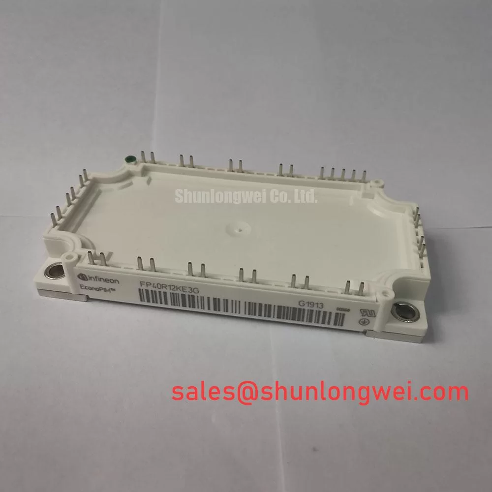
In high-voltage utility-scale conversion architectures, such as 1500V DC solar string and central inverters, the primary physical threat to semiconductor longevity is transient overvoltage during high-speed commutation. The FP40R12KT3G PIM (Power Integrated Module) from Infineon integrates a three-phase input rectifier, a three-phase inverter stage, a brake chopper, and an NTC thermistor into an optimized, compact footprint. With an inverter collector-emitter breakdown rating of VCES = 1200V and a nominal continuous current rating of IC nom = 40A at a case temperature of TC = 80°C, managing stray busbar inductance (Lσ) is an uncompromising engineering mandate.
During turn-off events under heavy fault current or steep load steps, the transient collector-emitter voltage spike is defined by the fundamental relationship:
Vpeak = VDC + Lσ × (di/dt)
When operating off an 800V to 1100V intermediate DC-link bus, a di/dt transition exceeding 2.5kA/μs will easily generate an overvoltage spike exceeding the absolute maximum silicon breakdown limit of 1200V if total loop inductance is not strictly controlled below 20nH. Achieving this demands wide, planar laminated busbars where the DC+ and DC- copper planes are separated by thin insulation films (typically 0.2mm to 0.5mm of high-dielectric Kapton or Nomex), maximizing mutual magnetic cancellation.
| Functional Block | Parameter Description | Symbol | Official Datasheet Value |
|---|---|---|---|
| Inverter Stage (IGBT) | Collector-Emitter Breakdown Voltage | VCES | 1200 V |
| Inverter Stage (IGBT) | Continuous DC Collector Current (TC=80°C) | IC nom | 40 A |
| Inverter Stage (IGBT) | Collector-Emitter Saturation Voltage (Typ) | VCE sat | 1.80 V |
| Thermal & Mechanical | Thermal Resistance, Junction to Case (IGBT) | Rth(j-c) | 0.60 K/W |
| Rectifier Stage | Repetitive Peak Reverse Voltage | VRRM | 1600 V |
| Brake Chopper Stage | Maximum DC Forward Current | IC | 40 A |
| Internal Sensor | Integrated Thermistor Resistance (25°C) | R25 (NTC) | 5.0 kΩ |
To further suppress parasitic turn-off oscillations, high-frequency polypropylene film snubber capacitors must be installed as close as mechanically possible across the module DC input pins. For systems requiring substantially higher output current handling in complementary stages, engineers often evaluate parallel multi-chip configurations or larger modules such as the FF800R12KL4C to maintain symmetrical current sharing without overloading single-die junctions.
💡 Bench Tip: During incoming inspection on the test bench, always ground yourself using a dissipative ESD wrist strap before handling the FP40R12KT3G. Verify the cold-state forward voltage drop across all six anti-parallel freewheeling diodes using a calibrated 6.5-digit multimeter in diode-check mode. At 25°C ambient, expect a standard forward drop between 0.95V and 1.25V at 1mA test current. Any deviation exceeding ±8% across the six branches indicates internal bond-wire variation or cell degradation.
PCB Gate Loop Layout Symmetry & Kelvin Emitter Routing Optimization
The switching dynamics of the IGBT trench-fieldstop cell inside the FP40R12KT3G depend heavily on gate drive loop inductance and gate-emitter path isolation. Parasitic mutual coupling between the high-current power emitter trace and the low-voltage auxiliary gate drive return introduces an induced voltage, eL = -LE × (di/dt), which counteracts the applied gate drive signal, causing uncontrolled switching deceleration, elevated turn-on losses, and dangerous parasitic turn-on due to Miller capacitance (Cres).
Implementing a dedicated auxiliary Kelvin emitter connection directly from the internal module pin to the gate driver IC output stage isolates the control loop from the high-power emitter path. The forward gate trace and the Kelvin emitter return must be routed on adjacent PCB layers as a tightly coupled differential stripline pair to minimize enclosed loop area.
In high-power solar conversion architectures, inverter output stages are exposed to aggressive common-mode noise. Gate driver optocouplers or digital isolators must exhibit a Common-Mode Transient Immunity (CMTI) of at least 100kV/μs to prevent false logic states during rapid dV/dt switching transients. When replacing modules or upgrading inverter stages to higher capacity platforms, such as transitioning to a BSM400GA120DN2, designers must re-evaluate driver output impedance to maintain gate loop dampening without inducing gate-emitter voltage ringing.
Protection coordination at the input rectifier stage requires careful alignment between semiconductor high-speed fuses and the module rectifier diodes (VRRM = 1600V). The clearing integral of the semiconductor fuse must satisfy the strict coordination equation:
I2tfuse ≤ 0.7 × I2tSCR / Diode
This ensures that under a catastrophic DC-bus flashover or dead-short event, the upstream fuse clears the fault energy well within the safe explosion-containment boundaries of the package, preventing thermal rupture of the housing.
High-Speed Fault Management: V_CE(sat) Desaturation Sensing Circuitry
Under short-circuit conditions (Type I hard switching fault or Type II fault under load), the IGBT desaturates, causing the collector-emitter voltage to rise rapidly while carrying full short-circuit current. The FP40R12KT3G silicon design provides a short-circuit withstand time (tsc) bounded by its Short Circuit Safe Operating Area (SCSOA), requiring complete fault interruption within 10μs at a starting junction temperature of 125°C.
Desaturation sensing circuits must monitor the collector voltage via a high-voltage blocking diode tied to the gate driver detection pin. When VCE exceeds the programmed threshold (typically set between 6.5V and 7.5V) for longer than the blanking filter duration (typically 1.5μs to 3.0μs), the driver must initiate an immediate Two-Stage Soft Turn-Off (2S-STO).
⚠️ Field Alert: Standard hard turn-off during a desaturation event induces an extreme di/dt spike across the remaining circuit loop inductance. Without two-stage soft turn-off or active collector clamping, the resulting inductive kick will destroy the IGBT gate oxide and silicon junction instantly. Technicians conducting bench validation should reference standardized diagnostic procedures outlined in the Field Engineer’s Handbook for calibrated fault injection testing.
Discrete power stages and co-packaged diodes require similar voltage clamping discipline, as documented across official design guidelines for Infineon IGBT Discretes & Co-Pack Diodes. The typical collector-emitter saturation voltage of the FP40R12KT3G sits at a low VCE sat = 1.80V, minimizing continuous conduction losses while operating at switching frequencies up to 20kHz in PWM solar conversion stages.
Thermal Paste Degradation Prevention and Mechanical Clamping Torque Calibration
Thermal energy extraction from the silicon dies through the copper direct bonded copper (DBC) ceramic substrate to the aluminum heatsink governs the long-term reliability of power modules. The FP40R12KT3G features an IGBT junction-to-case thermal resistance of Rth(j-c) = 0.60 K/W. Any mechanical mounting error directly degrades this thermal interface, accelerating junction overtemperature failures.
Applying thermal interface material (TIM) requires precise screen printing or automated roller application to maintain a uniform wet film thickness between 50μm and 100μm. Excessive grease increases thermal resistance, while insufficient paste leads to air voids that act as thermal insulators. Baseplate curvature compensation requires a strict sequential torque tightening sequence using calibrated torque tools.
| Mounting Step | Tooling & Method | Target Torque Value | Mechanical Objective |
|---|---|---|---|
| Pre-Fixation (Step 1) | Calibrated Torque Screwdriver (Cross Pattern) | 0.5 to 0.7 Nm | Even grease spreading; baseline seating without baseplate warping. |
| Final Torque (Step 2) | Calibrated Torque Screwdriver (Cross Pattern) | 1.1 to 1.5 Nm | Optimal metal-to-metal contact pressure; eliminates microscopic air voids. |
| PCB Terminal Fixation | Controlled Soldering Iron / Wave Profiler | 260°C ± 5°C (≤ 10s) | Zero mechanical shear stress on internal module terminal pins. |
Real-time thermal monitoring of the module internal environment is handled via the integrated NTC thermistor. At an ambient temperature of 25°C, the nominal resistance across the NTC terminals measures R25 = 5.0 kΩ. On the QA test bench, reading this value using a high-impedance source provides a direct indicator of sensor integrity. In operating inverters, the controller uses the calibrated B-value curve of this thermistor to execute derating algorithms whenever internal heat-sink temperatures exceed safety thresholds, protecting the silicon dies from thermal runaway.