Content last revised on October 24, 2026
FZ1200R33KL2 Ratings and Initial Fault Assessment
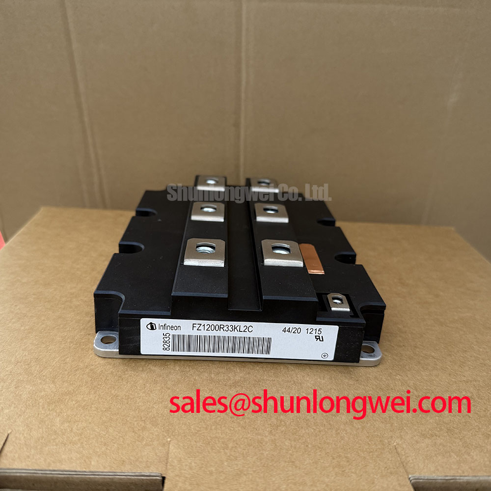
When a traction inverter reports an overcurrent or desaturation fault, isolate the power stage, discharge the DC link, and compare the suspect module with a known good switching path before applying test voltage. The Infineon FZ1200R33KL2 is specified for a 3300 V collector emitter voltage and a 1200 A continuous DC collector current at TC = 80°C. Its repetitive peak collector current is 2400 A for tP = 1 ms, while the specified operating junction temperature is −40°C to +125°C.
These ratings define the component boundary, not the complete operating limit of a traction converter. Bus voltage, switching energy, cooling resistance, gate drive behavior, commutation layout, fuse coordination, and protection timing must be assessed together. The specified junction to case thermal resistance is 0.015 K/W per IGBT and 0.025 K/W per diode. Those values are official component specifications and should be used with the complete thermal network, including the interface material, cooler, airflow, and transient thermal impedance data.
| Parameter | Symbol | Official Value |
|---|---|---|
| Collector emitter voltage | VCES | 3300 V |
| Continuous DC collector current at TC = 80°C | IC,nom | 1200 A |
| Repetitive peak collector current at tP = 1 ms | ICRM | 2400 A |
| Operating junction temperature | Tvj op | −40°C to +125°C |
| Junction to case thermal resistance per IGBT | Rth(j-c) | 0.015 K/W |
| Junction to case thermal resistance per diode | Rth(j-c) | 0.025 K/W |
Preventing Spurious Faults: Mitigating Hard Switching Transients in the FZ1200R33KL2
Hard switching faults should first be separated into gate drive malfunction, short circuit stress, commutation overshoot, and measurement error. During a controlled test, place the voltage probe reference at the intended measurement point and inspect the gate emitter waveform at the module terminals rather than at the distant driver board. A long probe return path can create ringing that appears to be a semiconductor fault.
A two stage soft turn off strategy is a Design Consideration for systems that must manage type I or type II short circuit behavior. The first response limits the immediate current transition, while the second response brings the device to the off state with controlled di/dt. Any proposed protection sequence should be checked against the manufacturer’s short circuit safe operating area and the actual desaturation detection delay. A response target below 10 µs may be used as a system engineering target only when supported by the applicable device data and verified during controlled testing; it is not presented here as an official FZ1200R33KL2 rating.
Minimize the commutation loop area and keep the gate return separate from high current emitter paths until the intended reference point. Clearance and creepage around the high voltage terminals should follow the converter insulation design, pollution environment, altitude, and applicable railway or industrial standards. The module itself should not be described as independently certified for the complete traction inverter EMC or safety system.
When a nuisance trip occurs, capture collector emitter voltage, collector current, gate emitter voltage, and the protection signal on the same time base. A clipped voltage waveform may indicate probe bandwidth or grounding problems, while an abnormal gate plateau may indicate driver saturation, excessive parasitic inductance, or a damaged gate circuit. The result should be compared with a controlled low energy switching test before the module is condemned.
Assembly Integrity and Layout Architecture: Diagnosing Latent Gate Emitter Dielectric Stress
Cold unpowered screening should begin with the main terminals isolated from the gate driver and DC link. With the gate held at emitter potential, use a digital multimeter diode check function to compare the antiparallel diode path in both polarities. Then check for an unexpected low resistance between gate and emitter using a meter whose test voltage stays within the module’s gate limits. These readings are comparative screening results, not substitutes for the manufacturer’s diode and gate leakage tests.
Any unexpected low impedance between gate and emitter, collector and emitter, or the diode path should be investigated alongside connector contamination, conductive thermal compound, loose busbar hardware, and moisture around the power terminals. A clean, dry assembly is particularly important in equipment that moves between heated depots and cold outdoor conditions. Condensation control belongs to the enclosure and maintenance program, not to the module rating alone.
Thermal assessment should account for switching frequency, load profile, coolant or forced air performance, and the transient thermal impedance of the IGBT and diode. A design review covering the intended switching frequency range is a Design Consideration when evaluating retrofit behavior, because conduction and switching losses change with operating frequency. The actual junction temperature must be checked against the specified −40°C to +125°C operating range under the worst credible duty cycle.
Inspect the heatsink contact pattern after removal rather than relying only on visual inspection. A localized dry area, surface contamination, uneven clamping, or aged interface material can raise case temperature and create intermittent protection events. ⚠️ Maintenance Note: Schedule heatsink cleaning and contact temperature checks with terminal torque verification before seasonal high load operation.
FZ1200R33KL2 Operational Boundaries: Evaluating Gate Drive Resistance When Replacing Legacy Modules
Retrofitting this 3300 V module into a legacy gate drive requires a measured comparison of turn on and turn off behavior. The external RG(on) and RG(off) values should be treated as system tuning components rather than fixed properties of the module. Increasing resistance can slow the transition and reduce ringing, but it can also increase switching loss; reducing resistance can improve transition speed while increasing voltage overshoot and electromagnetic disturbance.
Start with the legacy driver’s output capability, isolation arrangement, gate supply behavior, pulse width, and fault reset sequence. Then inspect the gate waveform directly at the module terminals during a low energy test. The waveform should be assessed for excessive oscillation, unintended plateau distortion, delayed turn off, and interaction between parallel switching positions. Final resistor values are system determined and should be validated against measured collector emitter voltage, current commutation, thermal rise, and protection timing.
Gate loop inductance should be minimized through a compact forward and return path, with the driver reference connected according to the module’s intended gate emitter topology. Avoid routing the gate loop beside high dV/dt collector conductors. If a legacy board cannot provide the required current or isolation behavior, replacing only the power module may not resolve the fault. A neutral comparison point for a related module is FZ1200R33KL2C, subject to mechanical, electrical, and gate drive compatibility checks.
Fast semiconductor fuses should be coordinated with the converter’s fault response and the protected circuit’s I2t characteristics. The fuse does not replace short circuit detection, and the module’s peak current rating should not be treated as a fuse selection value.
Benchtop Waveform Tuning: Mitigating Commutation Turn Off Voltage Stress
Commutation testing should focus on the freewheeling diode current transition, reverse recovery behavior, and the voltage overshoot seen at the power terminals. A high reverse recovery current or abrupt di/dt can interact with stray inductance and produce a collector emitter peak that is substantially different from the nominal DC link value. The evaluation must use a properly rated differential probe and a current measurement method that does not add a significant loop disturbance.
RC snubber selection is an Engineering Recommendation that depends on measured energy, parasitic inductance, switching frequency, and acceptable loss. Do not select the network from voltage rating alone. Test the snubber across the intended commutation path, observe resistor heating, and confirm that the added capacitance does not create an unsuitable turn on current or driver burden. Tailoring RG(on) can also reduce the aggressiveness of diode recovery, but the resulting switching loss must be included in the thermal calculation.
For pulsed operation, transient thermal impedance should be evaluated rather than applying only steady state Rth(j-c). The 0.015 K/W IGBT value and 0.025 K/W diode value are junction to case specifications; the peak junction temperature calculation also depends on pulse duration, duty cycle, case temperature, mounting interface, and cooler response. Use measured waveforms to establish the actual energy per pulse and verify the thermal margin against the specified operating junction range.
When the power stage includes a thyristor controlled front end, its gate trigger current and gate trigger voltage belong to the thyristor control circuit and must not be transferred to this IGBT module. Pulse train strength, isolation, and firing synchronization should be checked separately. For broader gate drive, thermal, and commutation layout reference, engineers can consult IGBT Design and Integration. Infineon’s public Intelligent Power Modules and CIPOS Nano IPM pages provide separate product family context and should not be treated as specifications for this module.