





Content last revised on September 10, 2026
Field Diagnostics & Commissioning: Long Motor Lead Reflected Wave Voltage in GD15PJX120F4S Topologies
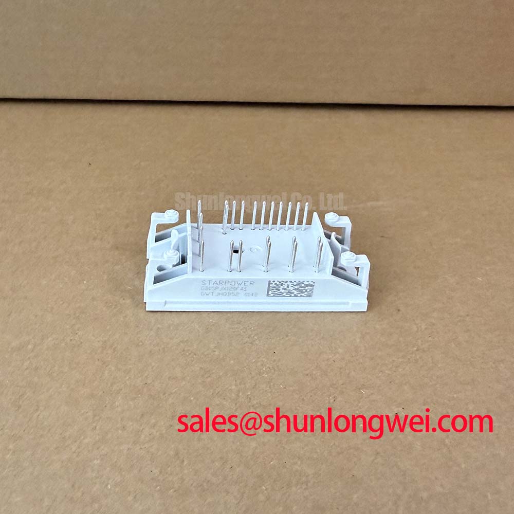
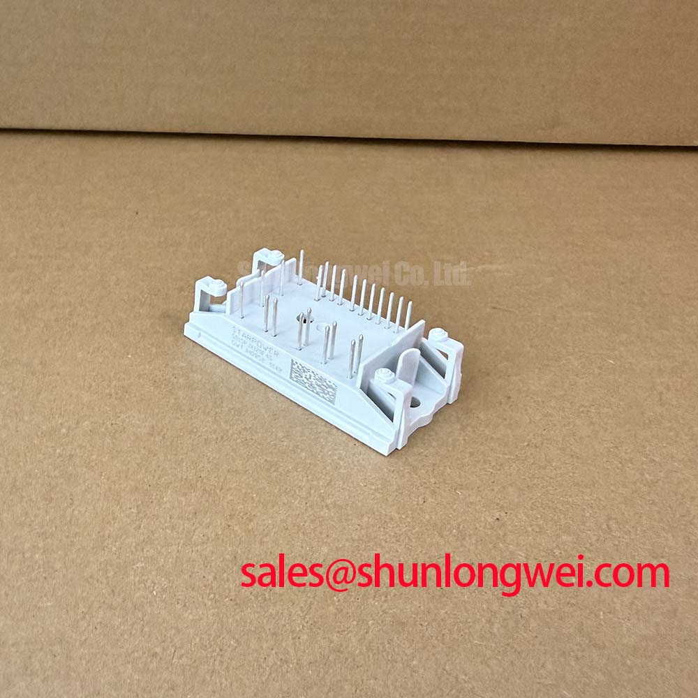
Check the module marking and perform a cold-state terminal inspection before energizing the equipment, then confirm that the replacement matches the original gate, collector, and emitter connections. The GD15PJX120F4S from StarPower is a 1200 V IGBT module specified for a continuous collector current of 15 A at Tc = 100°C. The supplied manufacturer data also lists a typical collector-emitter saturation voltage of 1.85 V, a short-circuit withstand time of 10 µs under the specified test conditions, and a typical IGBT junction-to-case thermal resistance of 0.85 K/W.
These ratings make the device relevant to engineering evaluations involving compact industrial inverters, motor drive outputs, regenerative braking choppers, and high-speed CNC spindle drive stages. Suitability remains dependent on switching frequency, cooling, DC-link conditions, overload profile, gate-driver behavior, and the complete power-stage layout.
| Parameter | Specified value | Engineering classification |
| Collector-emitter voltage, VCES | 1200 V | Official Specification |
| Continuous collector current, IC | 15 A at Tc = 100°C | Official Specification |
| Collector-emitter saturation voltage, VCE(sat) | 1.85 V typical | Official Specification |
| Short-circuit withstand time | 10 µs under specified test conditions | Official Specification |
| IGBT junction-to-case thermal resistance | 0.85 K/W typical | Official Specification |
| Gate-emitter threshold voltage, VGE(th) | 6.0 V typical | Official Specification |
Begin commissioning with the DC link discharged and the motor cable disconnected. Inspect the power terminals for contamination, looseness, and heat discoloration, then compare the gate and emitter reference wiring with the known-good inverter phase. The voltage rating of 1200 V is an official device limit, not a permission to accept uncontrolled switching spikes. A long motor lead behaves as a distributed electrical network, and impedance mismatch between the inverter output, cable, and motor can produce reflected-wave voltage at the motor terminals and at the IGBT switching node.
For a compact inverter or high-speed CNC spindle drive, measure the collector-emitter waveform with a properly rated differential probe and a short measurement loop. Probe placement should be close to the module power terminals because a remote measurement point can hide local overshoot caused by commutation inductance. The test engineer should record the DC-link voltage, turn-off peak, ringing frequency, gate voltage, and load current during acceleration, deceleration, and regenerative braking.
When the inverter absorbs regenerated energy through a braking chopper and power resistor, the chopper IGBT can experience repeated high-current pulses even when the average motor power appears moderate. The resistor, braking transistor, DC-link capacitor, cable inductance, and protection threshold must be assessed as one switching network. Designers should minimize the high-current commutation loop and verify the measured collector-emitter peak against the device rating under the hottest intended operating condition.
An output filter or motor choke may reduce cable-related voltage stress, but its selection is system-dependent. The engineer should verify its current rating, saturation behavior, switching-frequency loss, resonance behavior, and effect on spindle torque response. A filter that reduces the terminal edge rate can also alter switching-node waveforms and protection behavior. The neutral P546A2005 product reference can be reviewed when a parallel device evaluation is required, but electrical, mechanical, thermal, and gate-drive compatibility must be checked rather than assumed.
For fault investigation, compare the suspect phase with a known-good phase under the same DC-link and load conditions. Abnormal ringing may indicate parasitic inductance, probe error, cable mismatch, or gate-loop instability; it should be confirmed through repeated oscilloscope measurements rather than assigned to one cause from a single waveform.
Field Diagnostics & Commissioning: Baseplate Thermal Grease Layer Control in GD15PJX120F4S Topologies
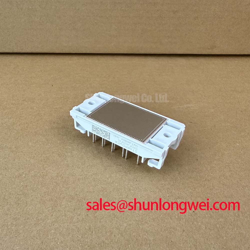
The stated typical junction-to-case thermal resistance of 0.85 K/W describes the IGBT thermal path to the case under the manufacturer’s specified test conditions. It does not describe the complete path through thermal interface material, heatsink, mounting hardware, enclosure, and airflow. During replacement, clean both mating surfaces using a process approved for the equipment and check the heatsink for burrs, contamination, and visible distortion.
A thermal interface layer should be continuous and thin enough to fill surface irregularities without creating unnecessary separation between the baseplate and heatsink. The frequently used 50 to 100 µm range is a general industry design consideration, not an official GD15PJX120F4S production specification. The correct application depends on the selected compound, surface flatness, pressure distribution, and the mounting instructions for the actual assembly. Excess compound can increase thermal resistance and contaminate nearby insulation or terminals.
Position the module without sliding it across the prepared surface, then tighten the mounting hardware in a gradual diagonal or manufacturer-defined sequence. Final torque must come from the module or equipment assembly documentation; a generic fastener value should not be presented as a StarPower rating. After installation, confirm that the baseplate is seated evenly and that the power terminals are not being used to pull the module into alignment.
Short-circuit protection requires coordination between the gate driver, current-sensing method, desaturation circuit, soft turn-off path, and system fault latch. The official short-circuit withstand time is 10 µs under the specified test conditions, but this value should not be treated as a target delay. A protection design may use a fast desaturation response and a controlled two-stage turn-off strategy, subject to driver capability and measured voltage overshoot. The engineer should verify the complete response time from fault recognition to gate-current reduction while checking that the soft turn-off event does not create an excessive collector-emitter transient.
Use the typical VCE(sat) value of 1.85 V as a reference for loss estimation, not as a guaranteed value at every current and junction temperature. During commissioning, compare the measured on-state voltage with the relevant datasheet test conditions and inspect thermal behavior at the actual duty cycle. Safety interlock note: discharge and verify the DC link before touching the module, gate driver, or braking resistor connections.
Benchtop Waveform Tuning: Mitigating Stress via Transient Thermal Impedance on GD15PJX120F4S
Static thermal resistance alone is insufficient when the GD15PJX120F4S is used in a braking chopper or a motor drive subject to pulsed overload. The junction temperature responds to the timing and repetition of each loss pulse. A transient thermal impedance network, commonly represented by several thermal resistance and capacitance sections, allows the test engineer to estimate how quickly heat moves from the semiconductor junction toward the case and heatsink.
Start with measured switching waveforms rather than relying only on nominal current. Switching energy should be evaluated from the actual voltage and current overlap, while conduction loss should use the measured or condition-matched VCE(sat). Apply the resulting pulse sequence to the relevant transient thermal model and compare the predicted junction excursion with the manufacturer’s allowable operating conditions. The calculated result is an Engineering Calculation, not a field-life guarantee.
At the bench, capture turn-on, turn-off, reverse-current commutation, and braking events over the intended speed range. A high-speed spindle drive can change its electrical operating point rapidly, so a waveform that appears acceptable at low speed may not represent the worst switching condition. Check the gate-emitter voltage directly at the module pins, keeping the power-current return separate from the driver reference wherever the package and board structure permit.
Gate-loop parasitic inductance can produce ringing, false gate movement, and Miller-related turn-on during the opposite switch transition. The recommended design principle is to keep the gate drive loop compact, route the return beside the gate path, and add damping only after observing the actual waveform. Gate resistance, turn-off bias, Miller clamp behavior, and any negative gate bias are system design choices that require verification against the driver’s absolute limits and common-mode transient behavior.
For regenerative braking, measure the DC-link rise and braking resistor temperature together with the IGBT waveform. A resistor that is correctly sized for average energy may still create demanding repetitive pulses if the control strategy permits frequent braking events. The thermal model should therefore use the real pulse spacing and cooling condition. The technical discussion in The Advanced Thermal Management Revolution provides useful background for evaluating thermal-path architecture, while the GD15PJX120F4S figures remain the controlling product data for this device.
Preventing Spurious Faults: Thermal Feedback Guidelines for GD15PJX120F4S
The typical VGE(th) of 6.0 V is a threshold reference measured under defined conditions, not a recommended drive level. A practical gate-driver evaluation should confirm the actual turn-on and turn-off voltages at the module terminals, the driver’s source and sink capability, and the response to common-mode ground movement. The auxiliary emitter or driver return path should be routed separately from the high-current power emitter path when the module’s terminal arrangement supports that practice.
Thermal feedback can influence protection thresholds and apparent current balance. The positive temperature behavior commonly associated with IGBT saturation voltage can assist static current sharing in suitably matched parallel arrangements, but dynamic balance is dominated by gate-loop symmetry, commutation inductance, driver propagation delay, and layout coupling. Designers should use matched gate-loop geometry and verify each device’s current and voltage waveforms with current probes and differential measurements.
Spurious desaturation faults should be investigated by checking the desaturation blanking behavior, diode path, sensing lead placement, gate voltage stability, and the timing relationship between the fault signal and soft turn-off. A fault indication may reflect a real overcurrent event, a transient measurement disturbance, insufficient noise immunity, or an unsuitable protection configuration. The correct diagnosis comes from correlating the fault signal with collector-emitter voltage, gate voltage, phase current, and DC-link behavior.
ESD handling is also part of gate-drive commissioning. The external protection process should follow the equipment’s controlled handling procedure and take account of recognized HBM, CDM, and MM concepts described in Electrostatic Discharge Protection Models. This reference does not replace the module’s manufacturer data or the system’s own qualification requirements.
When the power stage is used in a servo-oriented spindle system, the control engineer should assess the relationship between switching protection and motion response rather than changing fault thresholds in isolation. The operating principles described for servo drive precision motion control are relevant background for this system-level review. The final acceptance test should verify thermal response, switching margins, fault behavior, and motor performance under the intended inverter configuration.



