Content last revised on October 10, 2026
Benchtop Waveform Tuning: Mitigating Stress via Preventing Spurious Power-Up Shoot-Through on MG15G4GL1
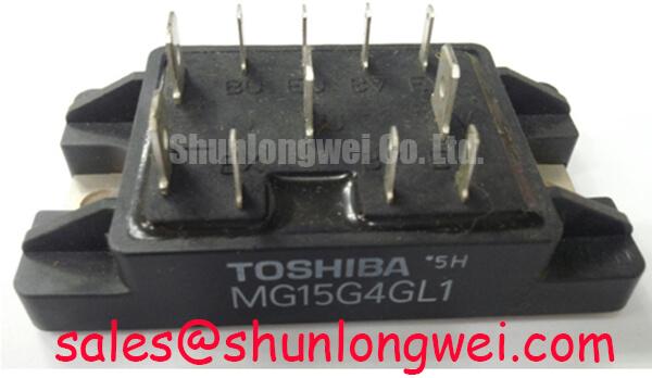
Check the inverter’s alarm history, isolate the DC link, discharge stored energy according to the equipment manufacturer’s procedure, and verify absence of voltage before using a meter to compare the replacement position with a known-good phase or removing the power module. The device specified for this service position is the Toshiba MG15G4GL1, an IGBT Module with a specified voltage rating of 1200.0 V and a rated collector current of 15.0 A under the manufacturer’s specified conditions.
For a compact industrial inverter or high-speed CNC spindle drive, these ratings define the primary component-identification boundary, not the complete operating limit of the finished converter. Confirm the original circuit topology, terminal markings, gate-driver arrangement, cooling path, and switching waveform before energizing the repaired assembly. The module’s control and protection behavior remains dependent on the surrounding driver, DC-link layout, load profile, and system interlocks.
Control the auxiliary driver supply before applying high-voltage DC-link power. A practical engineering recommendation is to keep the IGBT gate command in a defined off state while the driver supply rises, the undervoltage lockout becomes stable, and the controller confirms that both complementary switching commands are mutually interlocked. Where the driver architecture supports negative turn-off bias, designers may evaluate a negative gate level subject to the driver data, the module’s gate-emitter limits, and margin for gate-voltage transients.
Do not treat a clean low-voltage bench start as proof that the power stage is safe. Probe the gate-emitter signal and the collector-emitter node during controlled commissioning, using a measurement setup with suitable voltage ratings, common-mode capability, and a short connection loop. A brief gate pulse during auxiliary-power sequencing can create simultaneous conduction in complementary devices, producing a high-current shoot-through event before the controller has reached its normal operating state.
When a drive reports an overcurrent or desaturation trip immediately after power-up, separate the investigation into command timing and power-stage response. Compare the controller output, driver output, and module switching node in the same capture. A delayed gate transition, a floating input, an incorrect dead-time relationship, or an unstable UVLO release may each contribute to the observed event. The correct corrective action should follow the measured timing relationship rather than the alarm label alone.
Keep the high-current commutation path compact and physically separated from sensitive gate and fault-return wiring. This is a design consideration for limiting parasitic coupling and reducing false driver triggering; the final spacing and layout must be established against the enclosure, insulation system, working voltage, pollution environment, and applicable safety requirements. Long motor cables can also introduce reflected-wave effects and additional inverter loading, so the system engineer should assess the cable, motor, switching edge, and any output filtering together.
For a related system-level comparison, engineers evaluating a different Toshiba power-module position can review MG400Q1US41 as a separate device reference. It should not be treated as a drop-in substitute without checking electrical ratings, terminal arrangement, gate-drive compatibility, mechanical fit, and thermal conditions.
MG15G4GL1 Circuit Protection & Reliability: Calibrating Thermal Interface Material Thickness
Thermal installation begins with a flat, clean contact interface and a controlled thermal-interface layer. A 50–100 µm TIM thickness is a general design consideration, not an official MG15G4GL1 factory specification. The suitable thickness depends on the interface flatness, compound rheology, mounting pressure, baseplate condition, and the cooling assembly. Excess material can increase thermal resistance, while insufficient coverage can leave air voids beneath the module.
Inspect the mating surfaces for burrs, contamination, localized curvature, and previously hardened compound. Apply the material evenly and use a sequential screw-tightening method so that the baseplate settles progressively instead of being pulled down from one corner. The mounting hardware, washer arrangement, and final torque must follow the mechanical design and fastener specification used by the equipment manufacturer.
⚠️ Field Alert: Disconnect the DC link and driver supplies, discharge stored energy according to the equipment manufacturer’s procedure, and verify absence of voltage before touching the module terminals. Never insert or remove control wiring while the equipment is energized.
Terminal verification should be performed against the original equipment drawing and the module’s physical marking before any busbar is attached. Do not assume that a visually similar power module has identical collector, emitter, gate, auxiliary, or sensing connections. Check continuity and isolation with the module fully disconnected, using test methods and voltages suitable for the device, then confirm that the gate-driver return follows the intended emitter reference rather than an accidental high-current path.
Creepage and clearance are system-level insulation design considerations. Maintain the required separation around the high-voltage terminals, account for busbar edge geometry, and inspect for loose strands, flux residue, metal debris, and displaced insulating barriers. Vibration-resistant busbar fastening should prevent movement without transferring excessive mechanical load into the module terminals. After assembly, inspect the busbar for witness marks and verify that the fastening sequence has not altered the thermal contact.
The upstream rectifier and DC-link network also influence the module’s stress. During a topology review, MG300Q1US41 may be examined as a separate related power-device reference. Its suitability for any circuit position, electrical coordination, protection timing, and mechanical interchangeability must be assessed from the actual equipment design.
Transient Dynamics & Electrical Design: Thermal Time Constants and Peak Junction on MG15G4GL1
Evaluate pulsed overloads through the complete junction-to-case thermal path rather than relying only on the steady-state heatsink temperature. During a short overload, the junction temperature can rise faster than the case temperature, while the case and heatsink continue responding through slower thermal time constants. A multi-RC thermal model is useful when the manufacturer provides the required transient thermal impedance data; the calculated junction temperature should then be compared with the applicable device and system limits under the actual pulse width, duty cycle, case temperature, and cooling condition.
Where the necessary transient thermal curves are available, engineers can represent each thermal section as a resistance and time constant, then sum the contributions from the applied power pulse. This is an engineering calculation, not a substitute for the manufacturer’s specified safe operating area or short-circuit boundary. The test plan should capture collector-emitter voltage, current, gate-emitter behavior, case temperature, and fault timing so that an apparent thermal problem can be separated from switching overshoot or protection delay.
Desaturation protection and soft turn-off require coordinated validation. A short-circuit event can produce a rapid collector-emitter voltage rise and high instantaneous dissipation before the protection circuit reacts. The protection threshold, blanking interval, soft turn-off profile, gate resistance, and current-sensor response should be evaluated as one chain. Current measurement hardware used in inverter commissioning can be compared with the application information from LEM high-precision current transducers, while the operating context may resemble the high-current switching conditions discussed in welding power supplies.
For repetitive pulsed loading, the specified 15.0 A rating should not be interpreted as an automatic overload or surge allowance. Any short-duration collector-current limit or diode surge-current rating must come from the applicable manufacturer documentation and test conditions. The recovery interval between pulses, junction-temperature rise, gate-drive recovery, and protection reset all affect whether the next switching event occurs within a safe operating window.
Positive temperature coefficient behavior, where present at the operating point, can assist static current sharing when multiple compatible devices operate in parallel, but dynamic sharing remains sensitive to gate-loop inductance, driver resistance, layout symmetry, propagation delay, and thermal coupling. Parallel operation therefore requires matched current paths and oscilloscope verification during turn-on, turn-off, overload, and fault recovery. The Unlocking Efficiency in Industrial Drives technical guide provides broader context for switching-loss and industrial-drive design evaluation.
When the MG15G4GL1 is considered for a compact CNC spindle drive, verify the motor-cable length, output filter arrangement, braking path, fault response, and enclosure cooling as one integrated system. The module’s identity remains a Toshiba IGBT module with a 1200.0 V voltage rating and a 15.0 A collector-current rating under the specified conditions; final operating margins must be demonstrated by the assembled equipment under its measured switching and thermal conditions.