





Content last revised on September 30, 2026
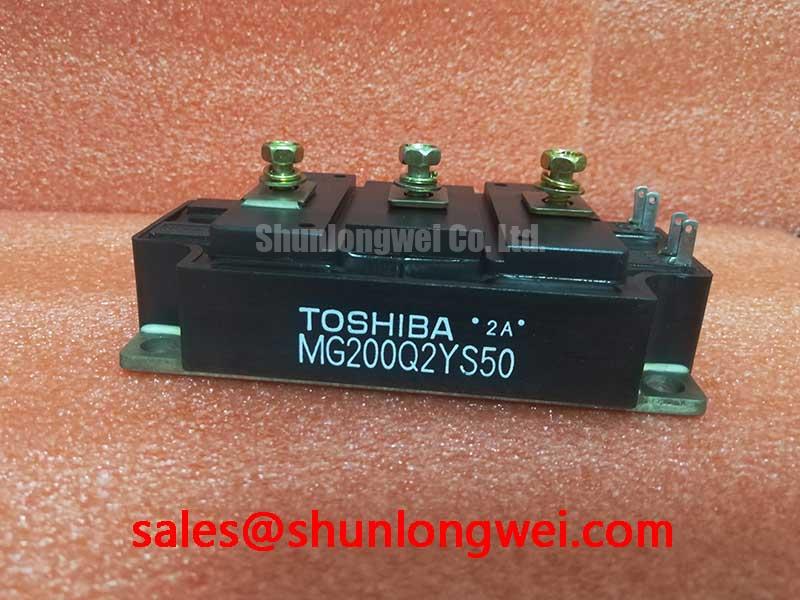
Benchtop Waveform Tuning: Checking the Gate Return on MG200Q2YS50
Probe the gate-to-emitter waveform at the module terminals during a controlled switching test, then compare it with the driver output to locate ringing or unwanted gate voltage rise. A clean driver signal does not establish a clean signal at the module: shared return impedance and wiring inductance can alter what the gate actually sees. The measurement reference matters, so keep the probe connection short and follow the equipment’s approved live-test procedure.
Trace the installed gate return from the driver schematic to the module terminals. A separate auxiliary emitter connection should be used for gate sensing only if the exact module terminal drawing confirms one; do not assign a terminal by resemblance to another Toshiba package. As a Design Consideration, separating a verified gate-sense return from the high-current emitter path can reduce coupling. The installer must still establish terminal identity, insulation spacing and routing from the equipment drawings before changing any connection.
If oscillation appears around a switching edge, compare the gate waveform with the collector-to-emitter waveform and the driver’s fault record. Review gate-loop routing, driver decoupling and damping together rather than treating a resistor change as a universal fix. Check complementary-switch dead time at the actual gate terminals: propagation delays and waveform tails determine whether the installed bridge avoids overlap. Review Miller-induced turn-on and any active-clamp function against the existing driver design, with settings established by system-level switching tests rather than assumed from the module’s voltage and current ratings.
Transient Dynamics: Assessing Voltage Stress on MG200Q2YS50
Capture the collector-to-emitter voltage at turn-off and compare its highest observed value with the 1200 V module rating (Official Specification). An elevated peak calls for inspection of the DC-link condition, commutation path, nearby capacitors and gate-drive behavior. Reducing parasitic loop inductance is a Design Consideration for limiting inductive overshoot; the acceptable layout and switching settings depend on measurements in the installed converter.
Altitude and terrestrial radiation can be relevant to high-voltage semiconductor reliability, but the MG200Q2YS50 specifications provided here do not establish a device-specific cosmic-ray failure rate, single-event-burnout rate or altitude derating curve. Do not calculate a FIT figure or assign a DC-bus derating from the 1200 V rating alone. For an installation with unusual environmental requirements, the equipment designer should evaluate those requirements using applicable manufacturer reliability information and the converter’s operating profile.
For a commercial string inverter or micro-grid energy-storage subsystem, treat the application as a compatibility assessment, not evidence of an approved fit. Compare the installed topology, DC-link operating range, fault handling, cooling arrangement and physical interfaces. ROHM’s IGBT technical resources provide broader context for IGBT technologies; they do not supply missing Toshiba device limits.
Preventing Spurious Faults: Inspecting Busbar Geometry and Protection
Inspect both sides of the commutation loop for loose joints, unequal current paths and snubber connections placed far from the switching terminals. During a controlled test, correlate a fault event with bus voltage, collector voltage and gate behavior. Turn-off overshoot rises with loop inductance and the rate of current change; that relationship explains why a compact, balanced current path matters, but it does not establish a universal inductance target or snubber value for this module.
As a Design Consideration, keep the positive and negative busbar paths closely coupled where the equipment’s insulation design permits, and connect any specified film snubber through a short current path. Verify electrical clearances against the original assembly design rather than narrowing them to improve a waveform. The system designer should select capacitor ratings and protection thresholds from measured switching stress and the converter’s documented operating limits.
Check the short-circuit protection chain as a coordinated system: driver detection, turn-off behavior, DC-link energy and the installed semiconductor fuse. A fuse’s current-squared-time characteristic must be assessed against the actual fault path and the module’s documented withstand limits; the 200 A current rating (Official Specification) cannot determine fuse coordination by itself. For related application context, see Industrial Applications.
When evaluating a replacement, compare the terminal map, mounting footprint, circuit configuration, cooling interface and driver requirements before comparing headline ratings. The SKM200GB12T4 comparison is useful cross-model context, not evidence that another module is a drop-in substitute for MG200Q2YS50.
Field Diagnostics and Commissioning: Checking the Thermal Path
Measure the cold-state terminal relationships with the DC link isolated and discharged, then compare readings across equivalent positions in the equipment before energizing the repaired assembly. Unexpected continuity or a marked difference from a known-good position warrants further isolation of the module, driver and connected buswork; a single meter reading does not identify the failed part. Inspect terminal seating, mounting flatness and the condition of the heat-sink contact area during the same shutdown window.
Field Alert: Verify the DC link is discharged before touching module terminals or disconnecting gate wiring.
During commissioning, log case or heat-sink temperature alongside load current and fault history. Case temperature cannot be converted into peak junction temperature during a pulsed overload without the module’s transient thermal-impedance data, loss information and a defined pulse profile. A multi-stage thermal model may support that calculation when those inputs are available; the 1200 V and 200 A ratings alone do not. Use the original assembly instructions for fastening and thermal-interface application, then verify cooling performance under a controlled load.
If paralleled switches are present in the equipment, inspect their shared buswork, individual gate paths and thermal contact rather than assuming equal current from matching nameplate ratings. Static current sharing and switching-time sharing require separate checks. Record the waveforms, temperatures and protection events at the load points used for the repair assessment so the equipment engineer can judge the commissioned assembly against its own operating limits.