


Content last revised on March 22, 2026
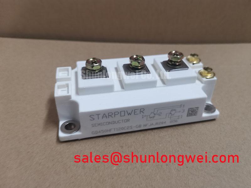
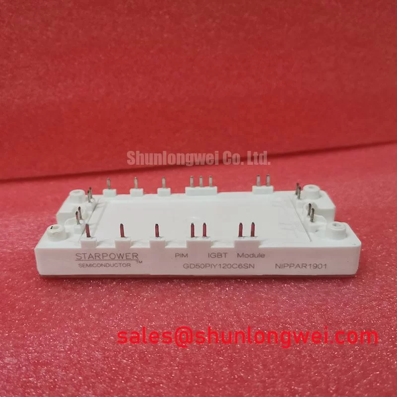
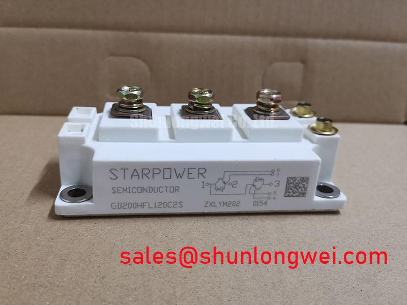
GD200HFL120C2S IGBT Module | Engineered for High-Frequency Power Conversion and Unmatched Efficiency
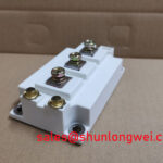
The GD200HFL120C2S is a high-performance 1200V, 200A half-bridge IGBT module designed for engineers pushing the boundaries of power density and efficiency. Optimized for high-frequency operation, this module provides a robust, thermally efficient solution for demanding industrial applications where every watt of lost energy impacts performance and operating cost.
Product Highlights at a Glance
- High-Frequency Optimization: Engineered with low switching losses (Eon, Eoff) to excel in applications operating above 20 kHz.
- Low Conduction Loss: Features a low collector-emitter saturation voltage (VCE(sat)), minimizing heat generation and improving overall system efficiency.
- Robust Half-Bridge Configuration: Integrates two IGBTs in a standard half-bridge topology, simplifying inverter and chopper circuit design.
- Integrated Anti-Parallel Diode: Includes a soft and fast recovery free-wheeling diode (FWD) co-packaged for optimal performance in hard-switching applications.
- Superior Thermal Performance: Built on a high-conductivity copper baseplate with an AlN substrate, ensuring excellent heat dissipation and reliability under heavy loads.
Technical Deep Dive: Beyond the Datasheet
The performance of the GD200HFL120C2S is rooted in its advanced semiconductor design. It utilizes a state-of-the-art Trench Field-Stop (TFS) IGBT structure. Unlike older planar designs, the trench gate architecture dramatically increases channel density, leading to a significantly lower VCE(sat). The "Field-Stop" layer is critical; it allows for a much thinner n-drift region, which not only reduces conduction losses but also slashes turn-off switching losses (Eoff) by enabling faster recombination of charge carriers. For a design engineer, this translates directly to lower cooling requirements and the ability to operate at higher switching frequencies without thermal runaway. For a deeper understanding of IGBT structures, explore our guide on deconstructing the IGBT.
Application Scenarios & Engineering Value
The unique characteristics of the GD200HFL120C2S make it a superior choice in specific high-stakes environments:
- High-Frequency Welding Power Supplies: In modern inverter welders, high frequency is key to achieving a stable arc and a compact design. The module's low total switching losses enable the design of smaller, lighter welding machines with precise current control for superior weld quality.
- Induction Heating Systems: Efficiency is paramount in induction heating. The low VCE(sat) and fast switching of this IGBT module minimize energy waste, reducing operational costs and allowing for higher power density in the converter, which is critical for rapid and uniform heating cycles.
- Solar Inverters and UPS: In the DC-DC boost and DC-AC inverter stages of solar inverters and Uninterruptible Power Supplies (UPS), every percentage point of efficiency matters. This module's optimized balance of conduction and switching losses maximizes energy harvest and extends battery runtime.
Key Parameter Overview
| Parameter | Value |
|---|---|
| Collector-Emitter Voltage (VCES) | 1200 V |
| Continuous Collector Current (IC) @ Tc=80°C | 200 A |
| Collector-Emitter Saturation Voltage (VCE(sat)) @ IC=200A, Tj=125°C | 2.1 V (Typ.) |
| Total Switching Energy (Ets) @ Tj=125°C | 19.5 mJ (Typ.) |
| Maximum Junction Temperature (Tjmax) | 150 °C |
| Short-Circuit Withstand Time (tsc) | 10 µs |
Frequently Asked Engineering Questions (FAQ)
1. What are the critical gate drive considerations for the GD200HFL120C2S to maximize its high-speed performance?
To fully leverage its speed, a carefully designed gate drive circuit is essential. We recommend a low-inductance layout, ensuring the driver is placed as close to the module as possible. Utilizing the auxiliary Kelvin Emitter pin provides a clean ground reference for the drive signal, bypassing voltage drops across the main power emitter connection. A robust gate driver capable of sourcing and sinking high peak currents (e.g., >10A) is necessary for rapid charging and discharging of the gate capacitance. Implementing a negative gate voltage (e.g., -8V to -15V) during the off-state is also highly advised to prevent parasitic turn-on induced by the Miller effect, especially at high dv/dt.
2. How does this IGBT module compare to a similarly rated SiC MOSFET for a new 50kW design?
This is an excellent application-dependent question. A SiC MOSFET will offer lower switching losses and higher operating frequency potential. However, the GD200HFL120C2S presents a more mature, cost-effective, and robust solution. Its short-circuit withstand time is significantly better than that of most SiC devices, offering a crucial layer of protection in rugged industrial environments. For applications operating in the 20-40 kHz range, the performance-to-cost ratio of this IGBT is often more advantageous. Our analysis on SiC vs. IGBT technology provides further context for this critical decision.
For detailed specifications, application support, or to discuss how the GD200HFL120C2S can fit into your next power project, please contact our technical team.