Content last revised on September 20, 2026
Field Diagnostics & Commissioning: Optimizing Heatsink Contact Pressure in GD300MLX65B3ST Topologies
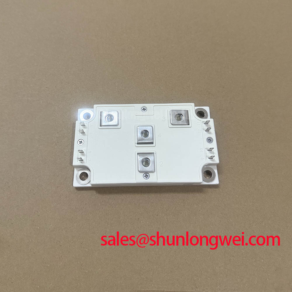
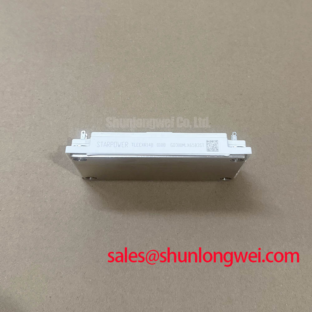
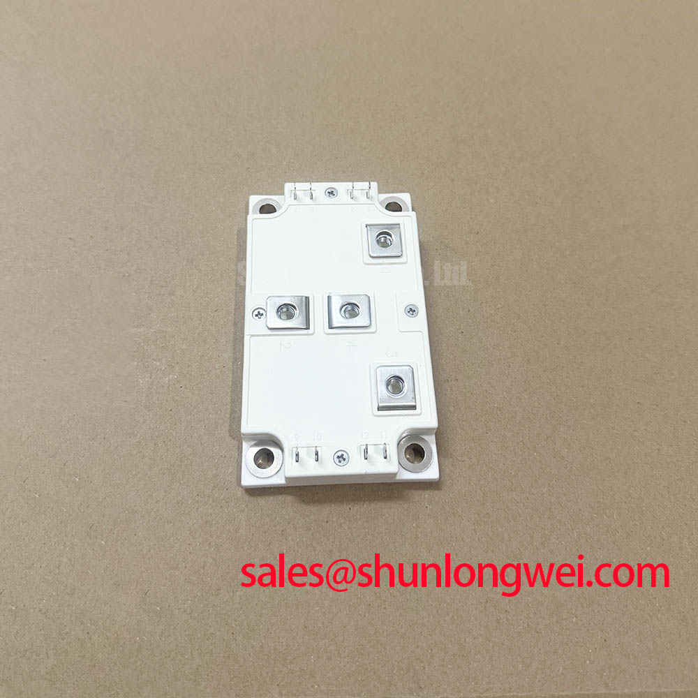
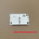
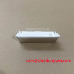
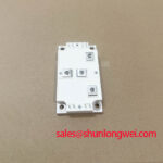
Before energizing a drive, isolate the DC link and compare the module terminal arrangement, cold resistance paths, control wiring, and mounting surface condition with the removed GD300MLX65B3ST assembly. This StarPower IGBT module is officially rated at 650 V collector emitter voltage and 300 A continuous collector current at case temperature of 100°C. Its published short circuit withstand time is at least 10 µs, the junction to case thermal resistance per IGBT is 0.14°C/W, and AC isolation voltage is 2500 V for one minute.
| Official Specification | Value |
|---|---|
| Collector emitter voltage, VCES | 650 V |
| Continuous collector current, IC at TC 100°C | 300 A |
| Short circuit withstand time, tSC | ≥ 10 µs |
| Junction to case thermal resistance per IGBT | 0.14°C/W |
| Isolation voltage, AC for one minute | 2500 V |
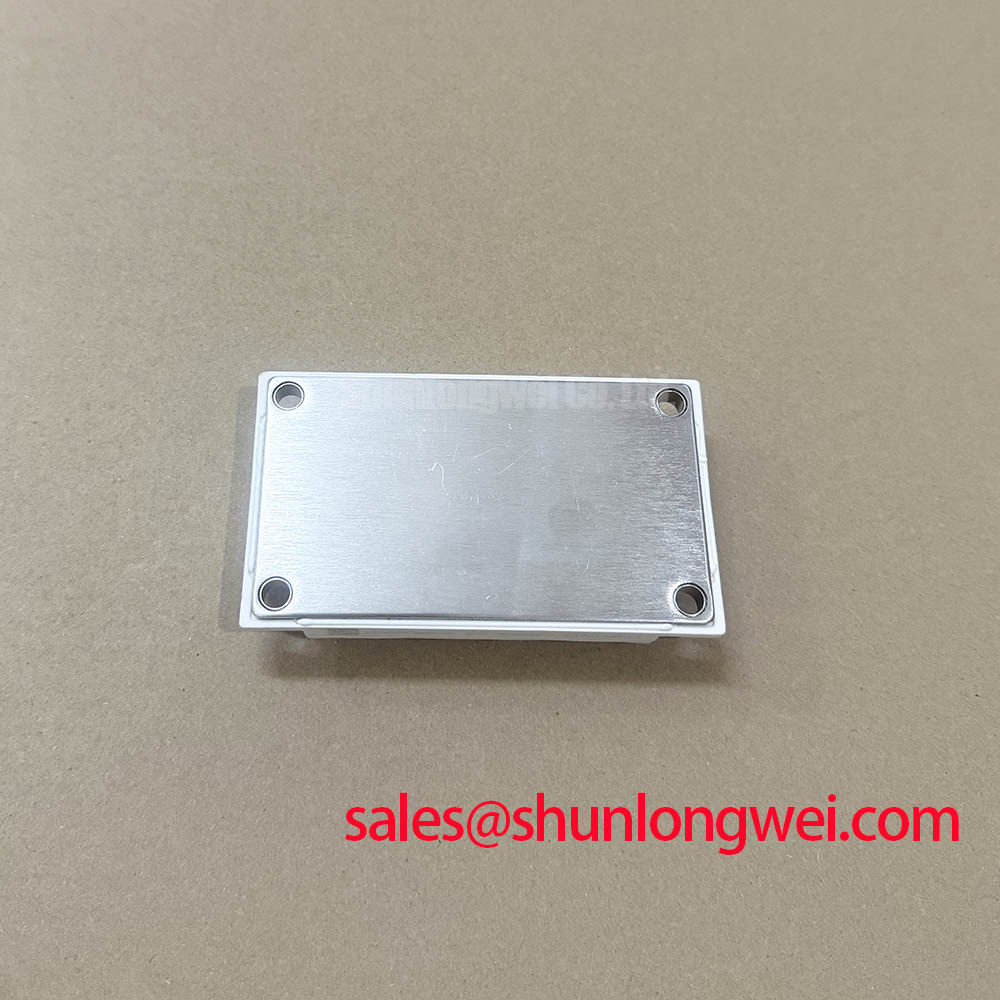
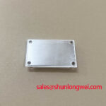
Start with the mechanical path because a sound gate driver cannot compensate for a poor thermal joint. Remove old thermal compound completely from the heatsink and module base contact area, then inspect for embedded debris, raised burrs, corrosion residue, or visible distortion. A contact pattern that is incomplete after removal can point to uneven pressure, a contaminated surface, or baseplate and heatsink flatness issues. It does not independently identify the cause, so the mounting stack should be checked before replacing active components.
The official 0.14°C/W junction to case thermal resistance per IGBT describes the semiconductor to module case thermal path. The system thermal result also depends on the thermal interface material, heatsink flatness, airflow, coolant performance where applicable, and clamp pressure. As a Design Consideration, use a controlled thin thermal interface layer, commonly within the general industrial handling range of 50 to 100 µm where the selected material and mating surfaces permit it. The objective is to fill microscopic surface variation without creating an insulating layer that increases thermal impedance.
Apply the interface material evenly and avoid trapping voids near the expected high heat flux region. Where a heatsink surface has slight curvature, contact should be assessed across the full base area rather than judged at one corner. Tighten mounting screws progressively in a cross pattern so that load is introduced evenly. The final torque must follow the module documentation, screw grade, heatsink thread design, and equipment assembly procedure; it is system determined and should not be inferred from the current rating alone.
⚠️ Field Alert: Do not fully tighten one mounting point before seating the others, because uneven clamp pressure can distort the thermal interface and produce misleading temperature behavior during commissioning.
On a stopped variable frequency AC motor drive, inspect the DC busbar spacing, phase terminal clearances, insulation barriers, and control connector retention before reconnecting power. The module’s 2500 V AC isolation rating for one minute is an official specification, but it does not replace equipment level creepage, clearance, enclosure, pollution degree, or dielectric test requirements. Designers should verify those conditions against the drive’s governing safety documentation and operating environment.
For a repair where the original module cannot be retained, electrical ratings alone are not a direct interchangeability statement. The related FP75R06KE3 can be evaluated as a separate repair candidate only after confirming terminal geometry, topology, gate drive arrangement, isolation requirements, thermal interface, switching behavior, and the complete drive documentation. A 650 V class marking does not establish physical or dynamic compatibility by itself.
GD300MLX65B3ST Thermal Electrical Optimization: Desaturation Detection Practical Tuning
Desaturation protection should be checked while the module is connected to the actual gate driver architecture, not as an isolated bench assumption. During normal conduction, the driver monitors the collector emitter behavior through its intended sensing network. If a short circuit or severe overcurrent condition causes the monitored voltage to rise abnormally, the protection path must command turn off within the practical protection window allowed by the application. The official tSC rating of at least 10 µs is a device capability specification, not a recommended blanking interval or a guaranteed system fault clearing time.
Type I and Type II short circuit events differ in their circuit origin and waveform development. A fault occurring while an IGBT is commanded on requires different observation from a fault created by a commutation event or external phase condition. In either case, designers should validate sensing delay, noise blanking, gate driver propagation, shutdown behavior, and measurement bandwidth on the assembled inverter. A desaturation signal that appears inconsistent may arise from switching transients, gate reference movement, probe placement, or an actual power stage fault. Capture the collector emitter and gate emitter waveforms against a known good channel before changing protection thresholds.
A controlled two stage soft turn off is a Design Consideration when the protection strategy must reduce abrupt current interruption. The purpose is to limit inductive overvoltage during fault clearing while still removing gate drive decisively. Its timing, gate impedance, clamp behavior, and permissible voltage excursion are determined by the DC link, motor cable, busbar layout, driver design, and measured switching response. The system engineer should verify peak voltage margin against the 650 V VCES rating during representative fault testing.
Phase angle control and line frequency ripple influence the current stress observed in a motor drive. When unexplained protection trips occur near torque transitions, inspect DC link ripple, current sensor alignment, phase current symmetry, and control timing together. An RC snubber may be considered where measured ringing indicates a transient problem, but its component values, losses, and thermal capability must be established from the actual waveform and switching frequency. The busbar loop should be made compact to reduce parasitic inductance and suppress turn off overshoot.
For broader diagnostic context on gate drive behavior, thermal paths, and system verification, consult the Power Electronics Masterclass. The article supports engineering review but does not replace the GD300MLX65B3ST application limits or the original drive design records.
Preventing Spurious Faults: Dynamic Braking Chopper Operation Guidelines for GD300MLX65B3ST
A rapid deceleration event can return motor energy to the DC link. If the braking chopper path, resistor assembly, control threshold, or associated wiring is compromised, the drive may report DC bus overvoltage, intermittent faults, or a braking related shutdown. These symptoms require measurement and inspection rather than a single cause assumption. Verify the DC bus waveform, braking command behavior, resistor continuity, thermal protection contacts, and power connections with the equipment safely isolated as required.
The GD300MLX65B3ST rating should be reviewed in the context of the complete inverter topology. It must not be assumed that this particular module contains a braking chopper IGBT or that it can directly replace an external braking switch. The system integrator should verify the original power schematic and module connection drawing. A braking transistor and ballast resistor must be selected and controlled according to the kinetic energy, deceleration profile, DC link limits, enclosure heat handling, and the equipment manufacturer’s protection scheme.
Keep braking loop conductors short and arranged to reduce loop area, particularly where the chopper connects between the DC link and resistor path. This is a Design Consideration intended to reduce switching disturbance and unwanted coupling into sensing circuits. Separate low level control routing from high current power paths where the cabinet layout permits, and confirm that shielding and reference connections follow the drive’s established architecture. A command signal that changes when the resistor circuit is energized can indicate coupled noise, reference movement, or a control board issue that needs waveform comparison.
Where an inductive auxiliary load is switched within the braking control circuit, a suppression component may be used according to the original design to control the stored energy released at turn off. The operating principle is described in this external reference on inductive kickback protection via flyback diodes. It should not be interpreted as a universal instruction to add a diode across a high power braking resistor or IGBT branch, since polarity, topology, voltage, energy, and switching requirements must be verified for the actual circuit.
During commissioning, observe the DC link and chopper gate signal with properly rated differential measurement equipment. Check whether the braking command, bus voltage change, and resistor current follow the intended sequence. This approach helps separate a control issue from a power connection or resistor bank issue without assigning fault responsibility to the module before evidence is available.
GD300MLX65B3ST Circuit Protection & Reliability: Calibrating Multi Module Parallel Current Sharing
When more than one power module is paralleled, static sharing and dynamic sharing must be treated as separate checks. IGBT conduction behavior can exhibit a positive temperature coefficient in relevant operating conditions, which can assist steady state current balancing. It does not guarantee equal current division across an assembled converter. Module temperature, contact resistance, DC bus geometry, gate path impedance, phase conductor length, driver propagation variation, and cooling distribution can all influence the result.
Use identical physical routing as far as the inverter construction allows. Each parallel branch should see comparable collector and emitter busbar paths, and each gate driver path should maintain matched reference behavior. A long shared emitter return or unequal gate loop geometry can cause one branch to switch earlier or later than the others, creating transient imbalance even if low frequency current appears acceptable. Minimize parasitic loop inductance to reduce turn off overshoot, then verify the measured peak conditions during switching tests rather than relying on geometric estimates.
For field troubleshooting, compare the same phase position across parallel branches under controlled load. Thermal imaging can identify a relative temperature difference, while current probes and differential voltage probes can show timing or waveform imbalance. A hotter branch may relate to reduced heatsink contact, altered gate drive, busbar resistance, uneven cooling, or a device related condition. Confirm mounting pressure, connector engagement, and gate path continuity before changing module positions or adjusting control settings.
The module’s official 300 A continuous collector current at TC 100°C applies to the stated device condition and should not be divided into a per branch system claim without a documented parallel design analysis. Likewise, the 650 V rating must be assessed against measured DC link voltage and transient behavior in the finished assembly. Parallel current sharing should be accepted only after the system engineer has verified thermal balance, dynamic switching behavior, protection response, and fault handling under the intended duty cycle.
Power cycling creates repeated thermal expansion and contraction within semiconductor assemblies and surrounding interconnect systems. This industry topic is explained in the external reference on power cycling and thermal fatigue in semiconductors. No operational lifetime figure can be inferred from that principle alone. For service work, focus on observable evidence: stable mounting, repeatable waveform behavior, consistent branch temperatures, and protection operation verified under controlled equipment conditions.