 IGBT basic application
IGBT It is a device composed of a MOSFET (input stage) and a PNP transistor (output stage). It has the characteristics of small driving power and fast switching speed (control and response) of MOSFET devices, and bipolar device saturation. The voltage is reduced and the capacity is large (the power stage is more durable), the frequency characteristics are between the MOSFET and the power transistor, and it can work normally in the frequency range of several tens of kHz.
IGBT turn-on process
The IGBT is divided into several periods during the turn-on process.
1. The turn-on process similar to MOSFET is also divided into three sections of charging time.
2. Only in the later stage of the drain-source DS voltage drop process, the PNP transistor adds a delay time from the amplification region to the saturation process.
In the above table, the definition is: turn-on time Ton, rise time Tr and Tr.i
In addition to these two times, there is another time for the turn-on delay time td.on:td.on=Ton-Tr.i
IGBT is in the shutdown process
During the turn-off of the IGBT, the waveform of the drain current becomes two segments.
The first segment is based on the characteristics of the MOS tube being turned off.
The second stage is that after the MOSFET is turned off, the charge stored on the PNP transistor is difficult to release quickly, resulting in a longer tail time of the drain current.
In the above table, the definition is: off time Toff, fall time Tf and Tf.i
Trv is the rise time of the DS terminal voltage and the turn-off delay time td(off).

The falling time Tf of the drain current is composed of two segments t(f1) and t(f2) in the figure, and the total off time can be called toff=td(off)+trv ten t(f), td(off The sum of +trv is also known as storage time.
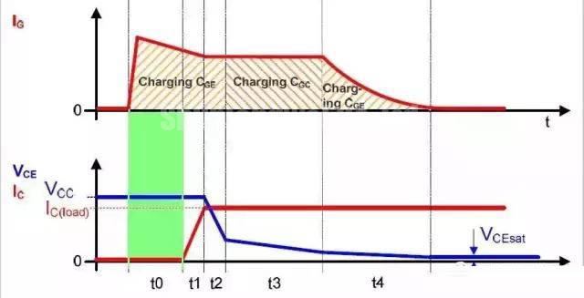
The detailed gate current and gate voltage, CE current and CE voltage can be seen from the following figure:
Looking at the MOS tube and IGBT tube gate characteristics from another picture may have a clearer concept:
Opening process
Try to calculate the turn-on process of the IGBT, mainly the heat dissipation of the time and gate resistance.
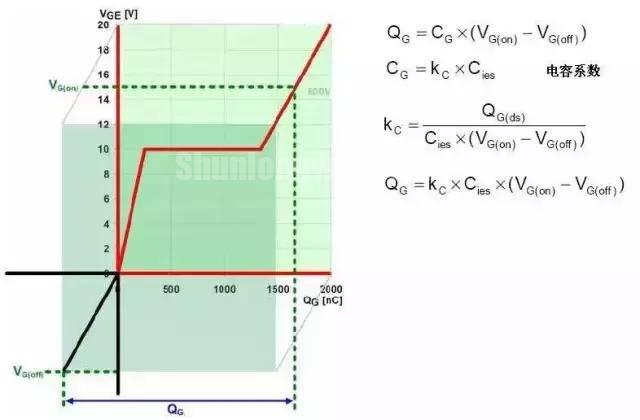
C.GE gate-emitter capacitance
C.CE Collector-Emitter Capacitance
C.GC gate level – collector capacitance (Miller capacitor)
Cies = CGE + CGC input capacitor
Cres = CGC reverse capacitor
Coes = CGC + CCE output capacitor
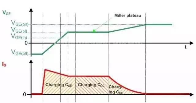
Phase 1:
The gate current charges the capacitor CGE, and the gate voltage VGE rises to the turn-on threshold voltage VGE(th). This process has a large current and can even reach a few amps of transient current. At this stage, the collector has no current and the pole voltage has not changed. This time is also the dead time. Since only the GE capacitor is charged, it is relatively easy to calculate. Because we use voltage source to supply power, This curve is indeed a first-order exponential curve.
Phase 2:
The gate current charges the Cge and Cgc capacitors, the IGBT starts to open, the collector current begins to increase, and the maximum load current IC is reached. Due to the reverse recovery current of the diode, the process of the MOS transistor is slightly different. Different, the gate voltage also reaches the Miller platform voltage.
Phase 3:
The gate current charges the Cge and Cgc capacitors. At this time, the VGE is completely unchanged. It is worth noting that the Vce changes very quickly.
Stage 4:
The gate current charges the Cge and Cgc capacitors, and as Vce slowly changes to a steady state voltage, the Miller capacitance also increases as the voltage decreases. Vge is still on the Miller platform.
Stage 5:
At this time, the gate current continues to charge Cge, the Vge voltage begins to rise, and the entire IGBT is fully turned on.
One of my colleagues is doing this to equate the whole process into a first-order process.
If this circuit is used as the drive circuit:
The equivalent circuit of the driver can be expressed as:
The power of time and resistance can be obtained by using the charge and discharge curves of RC.
In this case, it is equivalent to using the exponential curve instead of the whole ascending process, and the result is still somewhat different from the equivalent process.
However, because C.GE, C.CE, and C.GC are changing, and the voltage across the capacitor is changing at all times, we cannot completely sort out an idea.
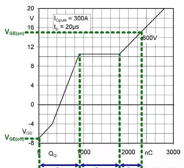
Many vendors recommend using Qg for calculations, and calculation methods can be sorted out. The only change is that Qg is measured under certain conditions. We don't know the tolerance of this approach.
The biggest problem with this approach is that the entire Tsw is used as the charging and discharging time, which is still somewhat doubtful.
Having said my personal opinion, it is very difficult to calculate the quantitative calculation of the whole time. In fact, the simulation is also the result of real-time calculation after digital modeling. This model may have a large comparison with the actual conditions. gap.
Therefore, if someone wants to calculate the entire gate control timing and time, it is ok to use a capacitor charging method to give a rough result. If it is accurate, it cannot be counted.
For gate-level resistors, each switch is transient power, and can be checked using the transient power of the previously described resistor.
Electrical impedance pulse capability
The size of the resistor we choose is to provide enough current, and also to be sufficient for its own heat dissipation.
The triode of the pre-stage, the speed of this triode is very fast, otherwise if the time to enter the saturation is not short enough, there may be a clamp when charging, so my opinion on this circuit is to be tested. Unloaded and loaded, there may be a big difference.
I have talked about some calculations in the front, and this time I summarize some design rules.
Gate Resistance: The purpose is to improve the slope of the rising and falling edges of the control pulse and to prevent parasitic inductance and capacitance oscillation, limiting the Sharp pulse value of the IGBT collector voltage.
The gate resistance value is small—charge and discharge are faster, which can reduce the switching time and switching loss, enhance the workability of the work, and avoid mis-conduction due to dv/dt. The disadvantage is that stray inductance in the circuit generates a large voltage spike on the IGBT, so that the gate is less susceptible to noise and is prone to parasitic oscillation.
The gate resistance value is large – the charge and discharge are slow, and the switching time and switching loss increase.
General: The positive gate voltage of 15V±10% is turned on, which can produce full saturation, and the switching loss is minimum. When the on-state loss is increased at <12V, it is difficult to achieve overcurrent and short circuit protection when >20V. The purpose of turning off the bias voltage -5 to -15V is that the noise can still be effectively turned off, and the optimum value of the turn-off loss can be reduced by about -8 to 10V.
The influence of the gate parameters on the circuit
The switching characteristics of the freewheeling diode inside the IGBT are also affected by the gate resistance and also limit the minimum value of the gate impedance we choose. The turn-on switching speed of the IGBT is essentially only compatible with the reverse recovery characteristics of the freewheeling diode used. The reduction in gate resistance not only increases the overvoltage stress of the IGBT, but also increases the overvoltage limit of the freewheeling diode due to the increase in di/dt in the IGBT module.
Gate resistance and turn-off change diagram
Gate-driven printed circuit board layout requires great care. The core issue is to reduce parasitic inductance, to prevent potential oscillations, reduce gate voltage rise rate, reduce noise loss, reduce gate voltage requirements, or reduce gate protection circuitry. Efficiency has a big impact.
Measure
Therefore, the leads driven to the gate are thickened to minimize the parasitic inductance between them. The control board and the gate drive circuit need to prevent inductive coupling between the power circuit and the control circuit.
When the control board and the IGBT control terminal cannot be directly connected, consider using a twisted pair (2 rpm / CM less than 3 CM long) or a strip line, and the coaxial line is connected.
Gate protection
For the sake of safety, a gate clamp protection circuit such as TVS can be used, and it is considered to be placed near the gate and emitter control terminals of the IGBT module.
Coupled interference and noise
The IGBT switches will use mutual potential changes, and the PCB boards should not be too close to each other. Excessive dv/dt will generate coupling noise from parasitic capacitance. To reduce parasitic capacitance between devices, avoid coupling noise.
Since power devices such as IGBTs have a certain junction capacitance, the delay of turning on and off the device may occur. Although we try to reduce this effect (increasing the gate drive voltage and current, setting the junction capacitance release loop, etc.). However, in order to prevent the off-delay effect from causing the upper and lower arms to pass through, because one bridge arm is not completely closed and the other bridge arm is in conduction state, the consequences after passing through the module are very serious (the best result is overheating).
Dead time (no load time) setting
In the control, the upper and lower arms are manually added and the time is turned off to ensure the safety of the drive. The dead time is large, the module work is more reliable, but it will bring distortion of the output waveform and reduce the output efficiency. The dead time is small, the output waveform is better, but it will reduce the reliability, generally us level, the typical value is above 3us.
In the application, it is especially important to note that the ambient temperature has a great influence on the toff, which makes the toff extended, and the addition of the gate resistor is also affected by the turn-off time, so adjustment is needed.