

Content last revised on September 21, 2026
Preventing Spurious Faults: Evaluating Thermal Capacitance vs Heat Sink Guidelines for J2-Q05B-G
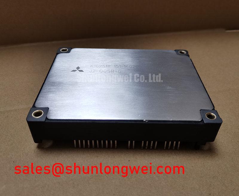
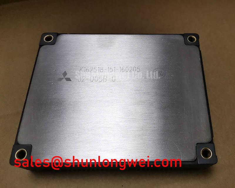
Begin a service inspection by checking the nameplate electrical boundary, examining the power transistor module for cracks or discoloration, and measuring the disconnected terminals against a known-good reference before applying DC-link power. The J2-Q05B-G is identified by the supplied manufacturer data as a Fuji Electric Power Transistor Module with an official rated voltage of 600.0 V and an official rated current of 5.0 A. These ratings establish the component identity, but they do not replace verification of switching frequency, pulse duration, duty cycle, case temperature, or the complete drive protection system.
For a replacement assessment in a heavy-duty variable frequency AC motor drive, the thermal path should be examined from the semiconductor junction through the module case, thermal interface material, heatsink, airflow path, and enclosure. A transient overload can produce a short electrical event without immediately producing a large heatsink temperature change. This difference between junction response and measured case temperature is a common reason that a drive can report an intermittent fault before a technician sees an obvious thermal symptom.
Official Specification: The available product data confirms the 600.0 V voltage rating, 5.0 A current rating, Fuji Electric manufacturer identity, and Power Transistor Module package classification. Detailed thermal resistance values, transient thermal impedance curves, allowable overload duration, switching energy limits, and junction temperature limits are not included in the supplied parameter set. Engineers should obtain the applicable original documentation before calculating a formal junction temperature margin.
| Parameter | J2-Q05B-G information | Engineering use |
|---|---|---|
| Manufacturer | Fuji Electric | Confirm against the original drive bill of materials |
| Rated voltage | 600.0 V | Compare with DC-link voltage and switching overshoot |
| Rated current | 5.0 A | Compare with RMS, peak, and overload current conditions |
| Package | Power Transistor Module | Verify terminal arrangement and mechanical fit before installation |
As a Design Consideration, a multi-section RC thermal model is more useful than relying on a single steady-state thermal resistance when the drive produces acceleration pulses, regenerative events, or repeated current peaks. The model should be populated only with manufacturer thermal data or measurements from a controlled test fixture. A technician can compare case temperature immediately after a fault with the drive’s current waveform, gate command, and fault timestamp. A mismatch between these records may indicate that the event is electrical, thermal, mechanical, or control-related rather than proving one single failure mechanism.
Thermal interface preparation deserves the same attention as electrical testing. The mating surfaces should be clean, flat, and free from foreign particles. Apply the selected thermal interface material as a controlled, continuous layer suitable for the surface finish and heatsink design. The final layer thickness and mounting torque are system and hardware dependent; use the module manufacturer’s mechanical instructions and the drive maker’s assembly specification rather than treating a generic value as an official J2-Q05B-G limit. The heatsink should also be checked for blocked airflow, uneven contact pressure, and contamination near the cooling channels.
The thermal path can be reviewed alongside the guidance in The Advanced Thermal Management Revolution, which discusses broader thermal-management approaches. That material is an engineering reference, not a substitute for the J2-Q05B-G datasheet or the drive manufacturer’s validated cooling design.
J2-Q05B-G Operational Boundaries: Evaluating Thermal Feedback Limits
When several power devices operate in parallel, static current sharing is influenced by the electrical characteristics of each device, the busbar resistance, emitter or source connection geometry, temperature, and gate-drive matching. The supplied product information does not provide a VCE(sat) curve, positive temperature coefficient data, gate-charge values, or parallel-operation approval for the J2-Q05B-G. Any claim about guaranteed current sharing therefore requires confirmation from the applicable Fuji Electric documentation.
As a Design Consideration, a positive temperature coefficient of conduction voltage can support static current balancing because a device carrying more current may experience a higher conduction voltage as temperature changes. That behavior must be verified across the actual current, temperature, and pulse range. It should not be used as proof that two modules can be paralleled safely under dynamic switching conditions. During evaluation, measure the collector-emitter waveform and current in each branch separately, using probes and current sensors appropriate for the switching environment.
Dynamic balance depends heavily on physical symmetry. Gate-loop conductors should follow comparable routes, with similar impedance and return paths. The power bus should avoid forcing one module to carry a different commutation path from another. Minimize parasitic inductance in the high-current loop and keep the gate-drive return separated from noisy power-current paths where the drive architecture permits. The final layout must be validated through double-pulse or equivalent switching tests, checking gate voltage, collector-emitter voltage, branch current, and fault timing.
For a repair engineer comparing physical alternatives, the QM200HA-HK may be reviewed as a separate product reference. It should not be treated as a drop-in replacement based only on current or voltage values. Terminal geometry, gate characteristics, isolation construction, dynamic ratings, mounting dimensions, and the drive control scheme all require independent confirmation.
Current measurement also benefits from a carefully selected sensor location. A fluxgate-based measurement principle, described in the fluxgate reference, illustrates why low-drift magnetic sensing can be useful in precision DC-current measurement. This reference does not specify the J2-Q05B-G and does not establish suitability for a particular inverter. The engineer must select a sensor with bandwidth, insulation, accuracy, and installation characteristics appropriate to the test setup.
💡 Pro Tip: Keep parallel gate and power paths physically symmetrical, then verify branch-current balance with oscilloscope and current-probe measurements before relying on thermal feedback for sharing.
J2-Q05B-G Circuit Protection & Reliability: Calibrating Turn-Off di/dt Induced Vpeak Clamping
During turn-off, the voltage observed across a power transistor is affected by the DC-link voltage, commutation inductance, current fall rate, measurement-loop inductance, and the behavior of the clamp network. In engineering terms, the inductive contribution rises as stray inductance and current slew rate increase. This relationship is useful for interpreting a waveform, but it does not provide a universal clamp value for the J2-Q05B-G because the allowable switching overshoot must be checked against the complete official rating and operating condition.
Begin protection verification with a properly compensated high-voltage differential probe and a short measurement loop. Compare the waveform at the module terminals with the waveform at the DC-link capacitor. A large difference can point to commutation-loop inductance, probe placement, busbar geometry, or clamp placement. Repeat the measurement under controlled current and temperature conditions, recording gate voltage and turn-off timing at the same time.
A metal-oxide varistor can be part of an overvoltage absorption network, but its selection is a system Design Consideration. Its continuous operating voltage, clamping behavior, pulse-energy capability, ageing characteristics, and coordination with the DC-link capacitor must be evaluated together. An MOV should not be described as sufficient protection without an energy calculation and a switching test. RC or RCD networks may also be evaluated where their losses, parasitic effects, and placement are compatible with the converter design.
The protection loop should be compact and symmetrical, with the clamp connected close to the commutation path it is intended to control. Do not impose an unverified inductance target on the layout. Instead, minimize the loop area, use a planar bus arrangement where practical, and confirm the resulting peak voltage through measurement. The system designer must determine the acceptable margin against the 600.0 V official voltage rating under the highest credible DC-link and transient conditions.
Insulation spacing also needs a physical inspection. Measure the actual clearance and creepage between high-voltage terminals, control wiring, heatsink interfaces, and grounded metalwork. The required distances depend on working voltage, pollution environment, material group, altitude, overvoltage category, and the applicable safety standard. The J2-Q05B-G parameter set supplied here does not define a certified insulation system or a complete creepage and clearance requirement. The equipment designer must validate these distances against the applicable product standard.
When the module is used within a rectifier and inverter topology, the 6MBI15L-060 can be reviewed as a separate rectifier-related reference. Compatibility depends on the complete DC-link voltage, charging circuit, control sequence, fuse coordination, and mechanical arrangement. No substitution or complementary pairing should be assumed from product naming alone.
J2-Q05B-G Thermal-Electrical Optimization: Long Motor Lead Reflected Wave Voltage Practical Tuning
Long motor cables can create transmission-line behavior, particularly when cable impedance and motor-terminal impedance differ significantly at the switching edge. The resulting reflected voltage may increase the stress at the motor terminals and at the inverter output stage. The magnitude depends on cable construction, length, switching edge rate, motor impedance, termination behavior, and the installed filter network. A general reflected-wave rule should therefore be treated as a Design Consideration rather than a guaranteed value for this module.
For a heavy-duty variable frequency AC motor drive, capture the voltage at the inverter output and at the motor terminals with suitable differential probes. The two waveforms should be time-correlated with phase current and gate command. If the motor-end waveform is substantially different from the inverter-end waveform, inspect cable routing, shield termination, grounding, output reactors, and the selected dv/dt filter. The evidence should come from measurement rather than from a single assumed cable-length threshold.
Output chokes and dv/dt filters can reduce edge stress, but they introduce voltage drop, additional losses, resonance possibilities, and control-loop effects. Their selection must be based on motor insulation requirements, carrier frequency, current waveform, thermal capacity, and the drive manufacturer’s approved configuration. The J2-Q05B-G’s official 600.0 V rating and 5.0 A rating do not define a complete long-cable filter recommendation.
At the module level, inspect the output terminals for signs of localized heating and verify that the mechanical connections remain secure after thermal cycling. Check the gate-drive signal at the module pins rather than only at the driver board, because connector inductance and return-path noise can change the waveform. If a drive trips only with a connected motor, compare the output waveform with a controlled load or approved test motor while maintaining the manufacturer’s safety procedure.
External references can help separate display or monitoring issues from power-stage faults. Truly Semiconductors Industrial Display Modules is relevant to industrial display and optical-interface technology, but it does not define the electrical or thermal behavior of the Fuji Electric power module. A service team should verify the display alarm through the drive’s stored fault code, measured DC-link condition, gate signal, and output waveform rather than assuming that a panel indication identifies the failed component.
Before energizing a repaired assembly, confirm terminal orientation, isolation condition, gate-drive interlock, precharge operation, protective fuse coordination, and the absence of unintended conductive paths. ⚠️ Field Alert: Disconnect and verify the discharged DC link before touching the module terminals, gate wiring, MOV network, or motor-output conductors.