


Content last revised on September 10, 2026
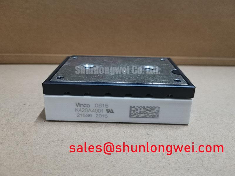
Preventing Spurious Faults: Symmetrical Busbar Geometry Guidelines for K420A4001
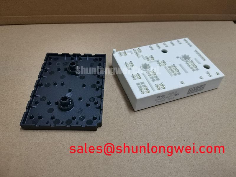
Begin the power-stage inspection with the physical current path. The positive and negative DC-link conductors should present comparable geometry to the commutation loop, while the phase output path should avoid unnecessary conductor length and abrupt changes in width. Symmetry is a design consideration rather than an automatic property of the module. It helps reduce unequal stray inductance, uneven current distribution, and differences in switching-node voltage seen by parallel paths.
For a three-level NPC or ANPC arrangement, the location of clamping devices, neutral-point conductors, and local DC-link capacitors should be reviewed together with the K420A4001 terminals. The 1200 V rating is relevant to device selection, but the complete switching cell determines transient stress. Designers should verify the peak collector-emitter voltage during double-pulse testing and under the worst combination of DC-link voltage, load current, temperature, and commutation direction.
Static current sharing can benefit from the positive temperature coefficient commonly associated with IGBT conduction voltage, but this should not be treated as a substitute for matched electrical paths. Dynamic sharing is strongly affected by gate-loop impedance, driver propagation mismatch, emitter-reference movement, and common-emitter inductance. Keep each gate-drive loop physically separated from the high-current collector and emitter path, and route the driver return to the intended emitter reference without allowing power current to share that conductor.
Dead-time control also requires measurement. Excessive dead time can increase diode conduction and switching loss, while insufficient dead time can allow cross-conduction during driver propagation mismatch. When troubleshooting unexplained overcurrent trips, capture both gate-emitter waveforms and the switching-node waveform with properly rated differential probes. Compare the timing of the known-good phase leg before changing protection thresholds or gate resistance.
💡 Pro Tip: Use a symmetrical laminated-busbar concept where practical, then verify turn-off overshoot and current balance with double-pulse testing rather than treating the layout geometry as proof of safe transient performance.
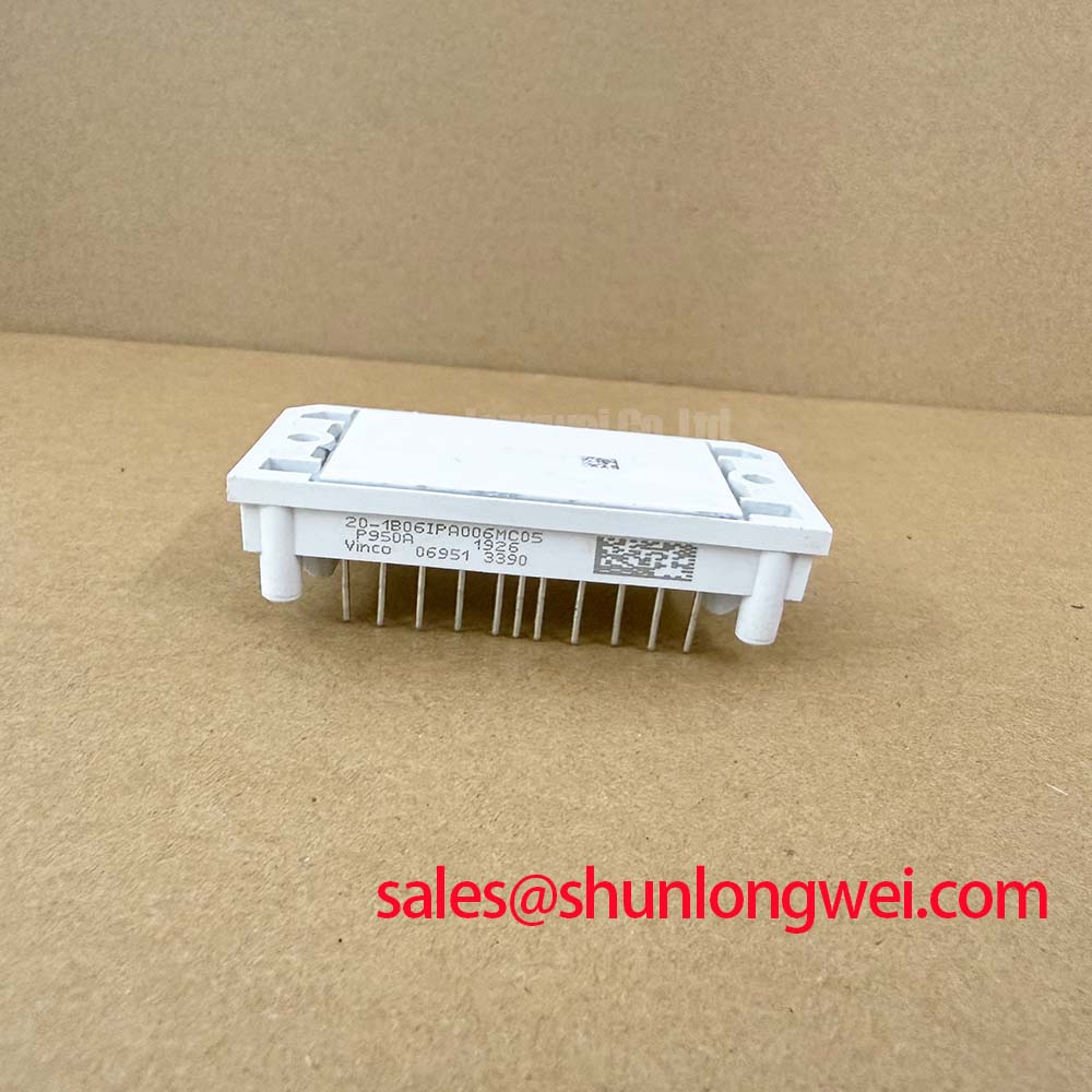
The P950A can be reviewed as a neutral comparison point during a sourcing study, but electrical compatibility must be established from the original system documentation and the relevant device data. Pin arrangement, thermal interface, switching behavior, and driver requirements should all be checked before considering any cross-reference.
K420A4001 Thermal-Electrical Optimization: DC-Link Capacitance Bank Layout and Low-ES Practical Tuning
Place the high-frequency portion of the DC-link capacitor bank close to the switching loop. Bulk capacitors may support stored energy and low-frequency ripple control, but their physical distance from the module can add commutation inductance. The resulting voltage excursion follows the normal relationship between DC-link voltage, loop inductance, and current slew rate; therefore, the system engineer must determine the peak voltage from measured switching waveforms and compare it with the K420A4001 voltage boundary.
Capacitor selection should consider equivalent series resistance, equivalent series inductance, ripple-current heating, temperature, aging behavior, and the frequency range of the switching event. A low-ES capacitor is not automatically the correct choice if its mechanical connection introduces a long or asymmetric current path. The positive and negative plates should connect to the switching cell with short, broad, and closely coupled conductors. Snubber capacitors, if required after measurement, should be positioned at the terminals that experience the observed transient rather than installed remotely as a general remedy.
The K420A4001 gate circuit should be assessed as a complete high-current loop. Gate resistance, driver output impedance, common-emitter inductance, Miller coupling, and the physical return path jointly determine ringing. The Miller plateau is influenced by the device capacitance conditions and the collector-voltage transition, so the required damping and active-clamp behavior are system determined. Confirm the gate waveform at the module terminals, not only at the driver output connector.
High-side driver power integrity is especially important in floating inverter positions. A bootstrap arrangement, where used, must be sized from the verified gate charge, driver quiescent current, switching duty cycle, refresh interval, leakage, capacitor bias characteristics, and temperature. Those values are not provided in the supplied K420A4001 parameter set, so the integrator should obtain them from the applicable device documentation before calculating capacitance or validating the driver supply margin.
Gate-drive isolation and power sequencing deserve the same attention as the power bus. Confirm that the driver supply reaches its valid operating region before enabling PWM, and verify that turn-off remains effective during an undervoltage event. The Evolution of Negative Off-Bias Gate Drive Circuits provides a useful reference when evaluating off-state noise immunity and negative gate-bias concepts. It should be treated as an engineering reference, not as a model-specific operating prescription.
K420A4001 Circuit Protection and Reliability: Evaluating Thermal Capacitance Against Heat Sinks
Thermal verification should start with the complete path from semiconductor junction to case, interface material, heat spreader, heat sink, and cooling medium. The module rating of 420.0 A is an official current specification, but the allowable operating point depends on conduction loss, switching loss, case temperature, cooling resistance, pulse duration, and the control strategy. Do not convert the current marking directly into a continuous cabinet current without a thermal calculation and test correlation.
For pulsed overloads, a single steady-state thermal-resistance value may not describe the temperature response. An engineering calculation can use a validated multi-RC thermal model to represent the short-term thermal capacitance of the semiconductor and case, then compare the calculated junction-temperature excursion with the device limits documented for the exact construction. The model should be checked against measured case temperature and electrical loss under representative current pulses.
Protection coordination should cover desaturation or overcurrent detection, gate shutdown behavior, DC-link discharge conditions, and fault energy. The detection circuit must distinguish a genuine switching fault from measurement noise, driver timing error, and a temporary commutation disturbance. A protection threshold should therefore be established from the actual short-circuit and overload capability documented for the device and driver combination, not from a generic IGBT rule.
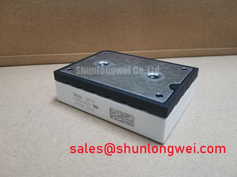
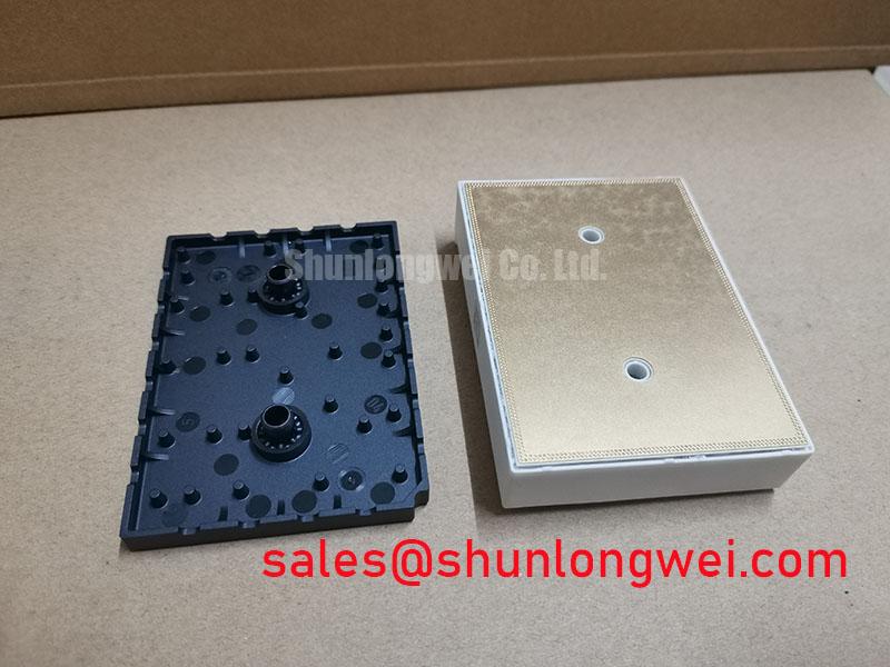
Inspect the mechanical thermal interface during service work. The isolated baseplate must sit evenly against the heat-transfer surface, with contamination, burrs, and uneven clamping removed before assembly. The interface compound and fastening method should follow the module manufacturer’s mechanical guidance. Avoid assuming that a familiar package torque or compound thickness applies to this model when the original installation documentation is unavailable.
For current measurement during transient testing, a properly installed current transformer, shunt, or Rogowski coil may be considered according to bandwidth, isolation, insertion loss, and calibration requirements. The Rogowski Coil Principle for Fast Transient Current Sensing explains the sensing principle, while the measurement setup itself still requires calibration against the intended current waveform. A current probe that saturates or has excessive loop area can obscure the event being investigated.
The Infineon IGBT Modules and Discretes Official Portfolio offers broader industry context for IGBT module terminology and application evaluation. It does not establish electrical equivalence with the Vincotech K420A4001.
K420A4001 Operational Boundaries: Evaluating Bidirectional DC-DC Buck-Boost Conversion Limits
In a bidirectional battery interface, evaluate the K420A4001 within the actual buck and boost commutation cells rather than assigning one universal current limit to both power-flow directions. A commercial micro-grid storage converter may move energy from a battery rack toward an inverter DC link during discharge and reverse the process during charging. Each direction changes the active switch, freewheel path, diode conduction interval, switching loss distribution, and thermal loading.
Four-quadrant operation also depends on control dead time, current-sensor polarity, gate-driver interlock, and the voltage range presented by both DC ports. Designers should verify that the 1200 V collector-emitter rating remains respected during regeneration, battery disconnect events, contactor transitions, and abnormal control states. The 420.0 A rating should be evaluated with the specified cooling conditions and the real current waveform, including ripple and overload duration.
For a system using a separate front-end rectifier or active input stage, the GD15PJX120F4S may be reviewed as a neutral complementary-stage reference. It should not be treated as an automatic pairing recommendation. The DC-link control loop, precharge circuit, protection coordination, isolation requirements, and semiconductor switching characteristics must be checked as one system.
Cyclic thermal swings during peak shaving can be evaluated by logging phase current, case temperature, coolant or heat-sink temperature, switching state, and ambient conditions over representative charge and discharge cycles. If thermal drift appears during only one direction of power flow, compare conduction intervals, gate timing, diode recovery behavior, and current-sensor alignment before attributing the condition to the module itself.
Layout clearance and insulation coordination remain system responsibilities. The integrator should verify terminal spacing, creepage, clearance, pollution environment, enclosure geometry, busbar edge treatment, and the applicable insulation test requirements for the finished converter. The isolated baseplate supports mechanical and electrical integration, but it does not by itself certify the complete equipment for safety, EMC, or environmental compliance.
During commissioning, begin with controlled DC-link energy, inhibited PWM, and instrumented gate and switching-node measurements. Increase operating stress only after confirming correct interlock behavior, stable gate-off voltage, balanced current paths, acceptable thermal response, and measured voltage margins under both buck and boost transitions.