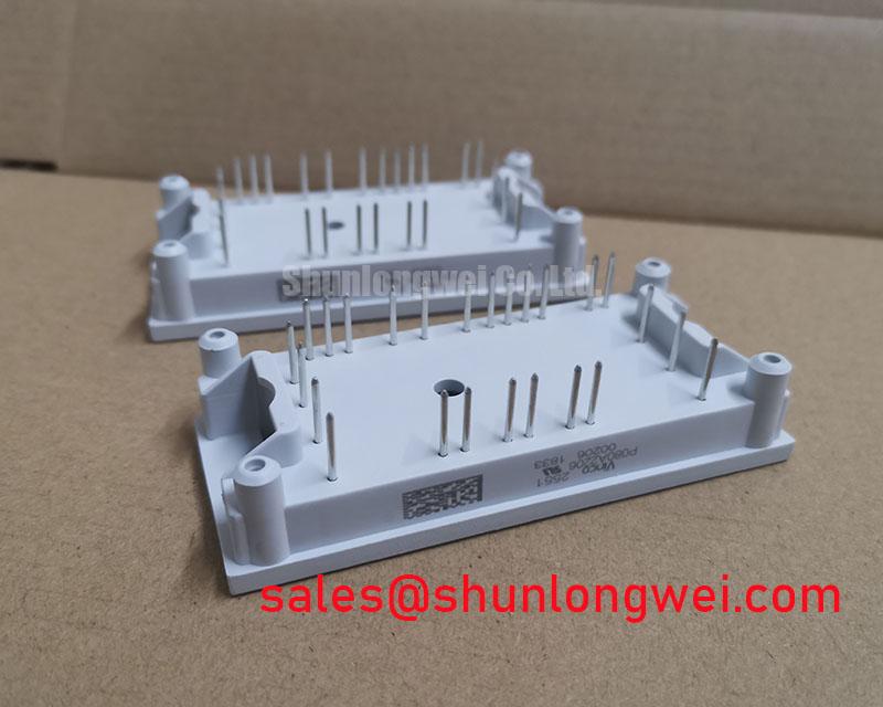
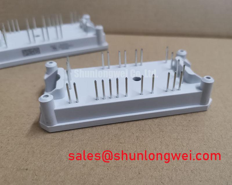

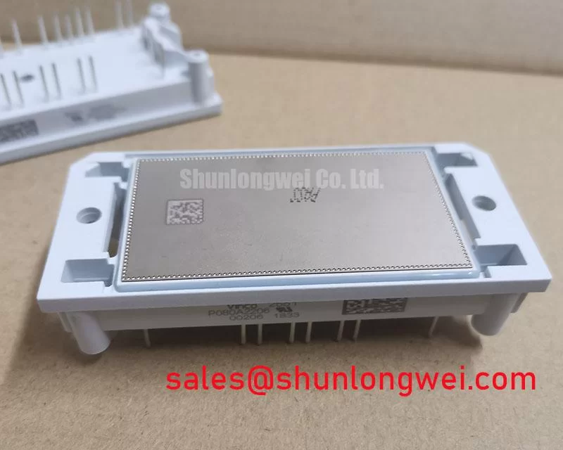
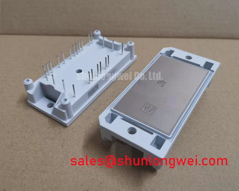

Content last revised on September 18, 2026
P080A2206 Thermal Electrical Optimization: Kelvin Emitter Connection Practical Tuning
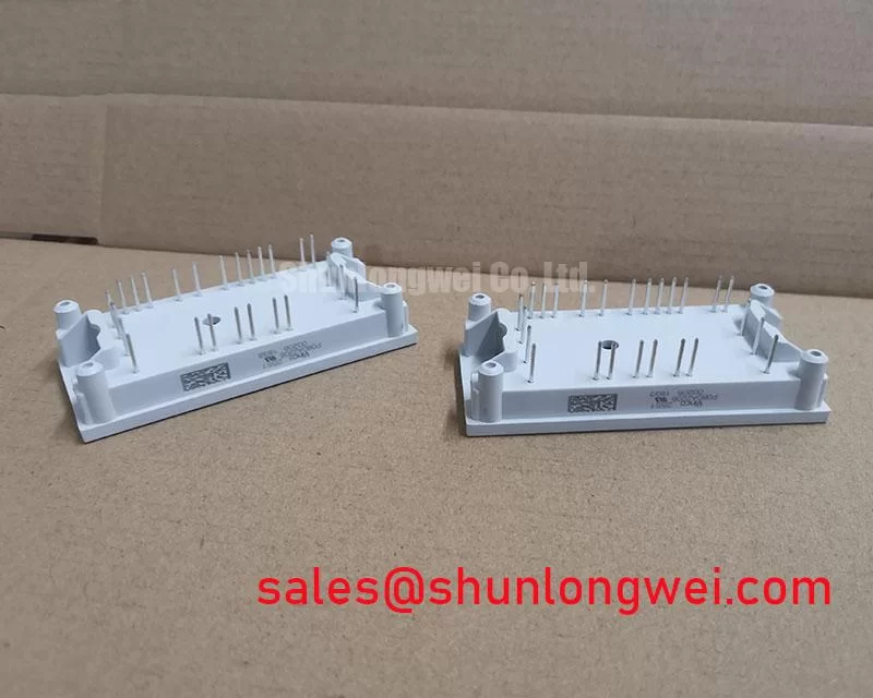
| Manufacturer | Vincotech |
| Part Number | P080A2206 |
| Product Category | IGBT Module |
| Rated Voltage | 2500.0 V |
| Rated Current | 80.0 A |
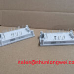
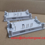
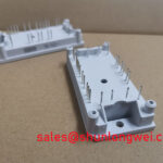
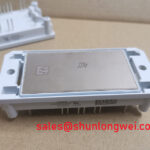
| Package | flowPIM / flowPACK |
Measure the gate to emitter path and inspect the main emitter and auxiliary return conductors for shared high current sections before applying a replacement module in a heavy duty variable frequency AC motor drive.
These checks help identify unwanted mutual coupling between the power emitter path and the gate driver reference. The published hardware data for P080A2206 confirms a 2500.0 V voltage rating, an 80.0 A current rating, and a flowPIM / flowPACK package, but it does not establish a universal external PCB layout, Kelvin terminal arrangement, or gate drive setting. The system integrator should verify the actual terminal functions from the original circuit documentation and the installed module drawing.
Design Consideration: keep the auxiliary emitter reference physically separate from the high current emitter return wherever the installed terminal arrangement provides that option. Route the driver return directly to its intended reference point, minimize the shared copper path, and avoid placing the gate loop beside the commutation loop for an extended distance. The clearance around high voltage terminals must also be assessed independently from the low voltage gate circuit, with creepage and electrical clearance selected for the working voltage, pollution environment, material group, altitude, and applicable equipment standard.
During field troubleshooting, compare the gate waveform at the module terminals rather than at the driver output alone. An abnormal turn off transient, repetitive gate ringing, or a change in switching behavior between parallel channels may indicate parasitic coupling or an unsuitable reference connection. Verify the signal with an isolated differential probe and compare it with a known good phase. The optical isolator or digital isolator must also be checked for common mode transient immunity under the actual switching conditions; the module itself cannot establish the CMTI performance of the complete driver board.
For a mechanically clamped power interface, inspect the flatness of both mating surfaces and confirm that the specified disc spring or washer arrangement has not lost its working position. The clamping method, bolt grade, contact surface, and thermal interface material are system assembly details, not published P080A2206 electrical ratings. ⚠️ Field Alert: isolate the drive and verify the DC link is discharged before disconnecting gate or power terminals.
For a neutral cross reference during urgent material planning, engineers can review P546A2005 as a separate compatible-device candidate, subject to complete electrical, mechanical, gate-drive, and thermal verification.
Preventing Spurious Faults: Transmission Line Impedance Mismatch Guidelines for P080A2206
Capture the collector emitter voltage and gate signal at the module terminals while the drive is operated at a controlled test condition, then compare the measured overshoot with the module voltage rating and the original design limits.
Long motor leads, cabinet bus bars, and poorly referenced probes can create transmission-line effects that make the measured terminal spike appear substantially higher than the local DC-link voltage. A possible approach is to evaluate the complete switching loop, including stray inductance, cable impedance, motor input characteristics, switching speed, and the DC-link capacitor location. Do not treat a claimed voltage multiplication as a fixed property of P080A2206; the resulting peak is installation dependent and must be verified by measurement.
Engineering Recommendation: minimize the high di/dt commutation loop and keep the gate drive loop compact, with signal and return paths routed together. When a motor cable is long or the motor has a high reflected-wave risk, the system designer should evaluate an output choke, dv/dt filter, or sine-wave filter. Filter selection depends on carrier frequency, motor insulation limits, cable length, leakage current, thermal dissipation, and the drive control strategy.
In rectifier and DC-link sections, phase-angle conduction control and line-frequency ripple smoothing influence the voltage presented to the inverter stage. Inspect the rectifier waveform, capacitor ripple current, busbar joints, and precharge circuit when unexplained overvoltage faults appear. A related topology reference may be found in SKM100GB063D, although its ratings and terminal arrangement must not be assumed to match this device.
RC snubbers, clamp networks, and MOVs can assist with transient energy management when selected for the actual circuit. An MOV should be coordinated with the continuous operating voltage, surge duty, clamping behavior, energy capability, fuse strategy, and required clearance. It should not be treated as a substitute for reducing commutation inductance. The final network requires bench validation with a correctly rated differential probe, thermal inspection, and repeated switching tests across the intended DC-link operating range.
P080A2206 Thermal Electrical Optimization: Thermal Feedback Practical Tuning
Compare the forward voltage behavior of each parallel current path at operating temperature and inspect the thermal interface, clamping surfaces, and gate waveform symmetry before attributing unequal current to the IGBT module itself.
IGBT conduction voltage commonly changes with junction temperature, and a positive temperature coefficient in the relevant operating region can support static current sharing between parallel devices. This behavior is not a substitute for measurement because the coefficient depends on operating current, junction temperature, gate conditions, manufacturing variation, and the specific device construction. The provided product data confirms the voltage and current ratings of P080A2206, but does not define a guaranteed parallel-current-sharing profile for a particular assembly.
Use symmetrical power paths where modules or switching positions are paralleled, and match the gate loop resistance, conductor length, driver reference, and local decoupling arrangement. Check each gate waveform at the corresponding module terminal. Unequal turn on or turn off timing can produce dynamic current imbalance even when the DC resistance and static voltage readings look similar. Oscilloscope measurements should be correlated with collector current, heatsink temperature, and the DC-link waveform.
Thermal inspection should include both sides of a clamped interface where the mechanical design uses double-sided cooling. Look for uneven contact marks, displaced thermal compound, warped contact plates, or a disc spring stack that no longer delivers the intended mechanical pressure. The correct pressure and installation torque must come from the applicable mechanical drawing and fastener specification; they cannot be inferred from the 80.0 A rating.
When operation involves high altitude or severe switching stress, designers should treat insulation coordination, partial discharge behavior, cosmic-ray-induced single-event burnout, and FIT expectations as application-specific reliability topics. No field failure rate, operating lifetime, or SEB margin should be assigned to this module without an authoritative test report or manufacturer reliability source. The practical task is to measure peak voltage, temperature, switching conditions, and insulation performance against the system requirements. The article Unlocking Efficiency in Industrial Drives provides additional system-level switching context.
For broader PIM topology comparison, consult the Fuji Electric Power Semiconductor and IPM Modules reference and its PIM Power Integrated Module information. These references describe related industry technology and do not alter the specified ratings of this Vincotech part.
Preventing Spurious Faults: Sizing Braking Resistors and Chopper Trans Guidelines for P080A2206
Measure the DC-link rise during the actual deceleration profile and confirm the braking chopper waveform, resistor temperature, and protection thresholds before changing the braking circuit around P080A2206.
The braking IGBT and ballast resistor must absorb the kinetic energy returned by the motor without exceeding the DC-link voltage, semiconductor switching limits, resistor pulse capability, or enclosure thermal limits. Resistor selection is therefore based on motor inertia, commanded deceleration, load profile, regenerative energy, duty cycle, allowable bus voltage, and the chopper control strategy. The 2500.0 V rating of the module is an official product parameter, not a recommended operating target for the complete braking circuit.
Inspect the chopper gate command and collector emitter waveform together. A delayed gate signal, excessive ringing, or a resistor that heats during light-load operation may point to control timing, sensing, wiring inductance, cooling, or an incorrectly coordinated clamp network. Check the braking resistor connections for looseness and verify that the resistor’s pulse and continuous ratings are appropriate for the measured energy profile.
Keep the braking commutation loop short and physically separated from sensitive speed feedback, gate signals, and communication wiring. Designers should verify peak voltage at the chopper terminals during the worst credible deceleration event, including a sudden stop, high-load regeneration, and mains disturbance. Any MOV, active clamp, or RC snubber used in this section requires coordination with the resistor pulse energy and the chopper switching frequency.
When replacing a failed unit, compare terminal geometry, insulation spacing, heatsink contact, gate-driver compatibility, and the original protection sequence rather than relying on voltage and current ratings alone. The system engineer should complete controlled no-load and loaded tests, then confirm thermal equilibrium and fault response before returning the variable frequency AC motor drive to service.