



Content last revised on September 20, 2026
Benchtop Waveform Tuning: Mitigating Stress via Dynamic Braking Chopper Operation on K209A4004
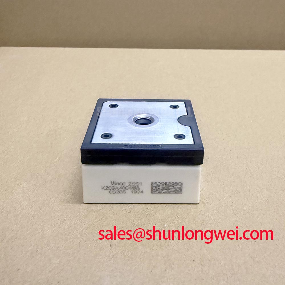
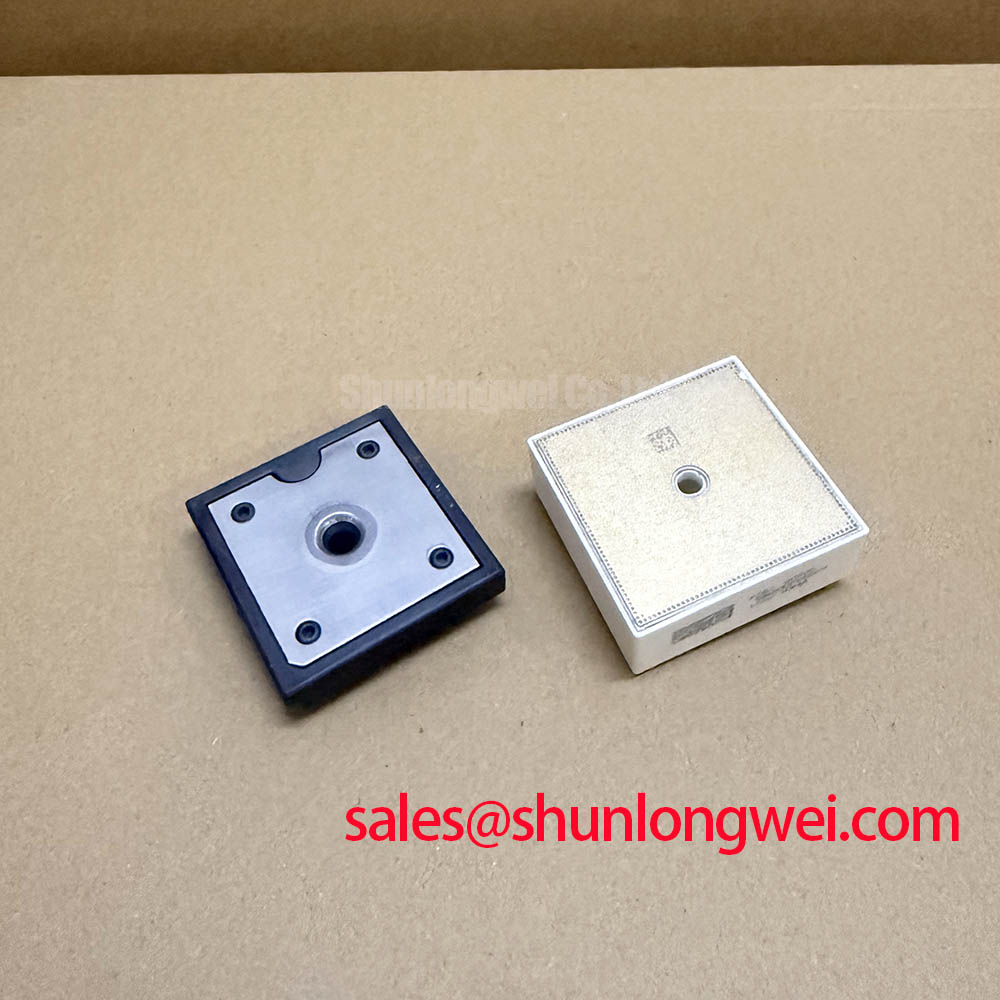
Before reconnecting a drive, verify that the equipment nameplate and circuit documentation identify a K209A4004 power stage, then isolate the DC bus and inspect the module terminals, busbar contact faces, gate wiring, braking resistor connections, and nearby suppression components for heat discoloration, loose hardware, or damaged insulation. The K209A4004 is a Vincotech Power Integrated Module with a Converter Inverter Brake topology. Its official ratings include 1200 V collector emitter voltage, 8 A continuous collector current at 80 C, and a 1600 V rectifier voltage rating.
In a forklift low voltage traction inverter, deceleration can return motor energy to the DC link. When battery acceptance, charging state, wiring resistance, or system operating conditions limit energy absorption, the braking function must transfer excess DC link energy to the braking resistor under control of the drive. The braking path should be evaluated as a system function, not as an isolated module feature. Verify the resistor condition, its thermal protection path, wiring integrity, controller command logic, and the measured DC link response during a controlled deceleration event.
For a braking chopper investigation, capture the DC link voltage, brake command, gate waveform, and braking current with measurement equipment referenced correctly to the power stage. A brake event that is absent, intermittent, or excessively noisy can arise from several interacting conditions, including control inhibition, an open resistor path, unsuitable gate drive behavior, busbar inductance, or a sensing problem. Comparing the captured waveform with a known good drive of the same design can help separate a module concern from a system control concern.
Design Consideration: Keep the braking current loop physically compact, with the DC link capacitor, braking path, and related conductors arranged to minimize parasitic inductance. This reduces inductive voltage overshoot during turn off, but the final layout margin must be verified by switching tests against the actual DC link voltage and operating load. A metal oxide varistor or other coordinated clamping network should be assessed only against the complete equipment transient environment and its approved protection scheme.
The integrated rectifier portion is specified with a 1600 V rectifier voltage rating. In systems where the front end, supply interface, or rectification arrangement is being assessed alongside the inverter, a related component such as P950A can be reviewed as a separate compatibility item. Its electrical ratings, terminal arrangement, thermal path, and circuit role require independent verification before any service decision.
Topology matters when tracing energy flow. A conventional forward converter, for example, has a different energy transfer and reset mechanism from a motor inverter braking circuit. Avoid applying voltage waveform expectations from one topology directly to the other. Use the original equipment schematic to establish which terminals carry rectified input, inverter phase current, braking current, and control signals.
K209A4004 Thermal Electrical Optimization: Derating Guidelines and Mismatched Parameter Practical Tuning
The official typical collector emitter saturation voltage for the K209A4004 is 1.9 V at 8 A and 150 C. This value is an official specification under stated test conditions, not a fixed loss value for every switching frequency, gate drive arrangement, temperature, or load waveform. In service analysis, compare phase current, heatsink temperature, cooling airflow, thermal interface condition, and switching behavior before attributing heating to the module itself.
The positive temperature coefficient associated with IGBT conduction behavior can support steady state current sharing in suitably matched parallel arrangements, but it does not establish dynamic current balance. Dynamic sharing is influenced by gate loop impedance, driver propagation timing, power loop symmetry, device condition, and the actual switching environment. When multiple current paths are present, engineers should verify each gate path and power connection with the same care given to the thermal assembly.
Design Consideration: A thin, uniform thermal interface material layer is generally used to avoid large voids while maintaining proper contact between the module baseplate and the heatsink. The selected material, surface flatness, pressure distribution, and original equipment service procedure determine the appropriate interface condition.
Mount the module on a clean, flat heatsink surface and tighten its fasteners in a cross pattern so pressure develops evenly across the baseplate. Use the module documentation and equipment service specification for the applicable fastener size and tightening requirement. Uneven clamping can produce an inconsistent thermal path even when the electrical circuit appears correct.
Field Alert: Do not power the inverter after replacing a power module until the gate connections, phase conductors, DC bus polarity, and heatsink fasteners have been independently checked against the original equipment documentation.
For replacement assessment, the physical footprint, topology, terminal designation, gate drive requirements, thermal interface, and protection coordination must all match the repaired assembly. A K420A4001 may be reviewed as a separate Vincotech module reference, but no cross model substitution should be assumed from part family naming or headline ratings alone. The system integrator should verify the original schematic and manufacturer documentation before establishing compatibility.
Assembly Integrity & Layout Architecture: Implementing DC Bus Operating Voltage Headroom Derating for K209A4004
The 1200 V VCES rating defines an official collector emitter voltage boundary for the K209A4004. It does not by itself state a permitted DC bus operating voltage for every inverter. The allowable operating point depends on switching overshoot, repetitive transient conditions, line disturbances, braking events, snubber behavior, cooling conditions, gate drive performance, and the protection response of the complete system.
Engineering Recommendation: Establish DC bus operating headroom through measured switching waveforms at relevant current, temperature, and supply conditions. The test should capture the peak collector emitter stress created by the actual power loop, rather than relying only on a nominal bus measurement. This allows the system engineer to confirm that transient behavior remains within the official device rating under the required operating envelope.
Keep laminated conductors or paired busbar paths close and symmetric where the equipment architecture permits. Short, direct paths between the DC link capacitor and the inverter power terminals reduce loop inductance and can help suppress turn off overshoot. Clearances, creepage paths, insulation barriers, and connector spacing must follow the equipment level voltage, pollution, enclosure, and applicable safety requirements rather than a generic module installation rule.
High altitude operation deserves a separate equipment level review. Terrestrial neutron flux changes with altitude, and semiconductor susceptibility can depend on device technology, blocking voltage, operating voltage, temperature, and actual mission conditions. No field failure rate, Single Event Burnout rate, or FIT value is asserted here because no K209A4004 manufacturer source has been provided for those conditions. Design Consideration: where equipment is deployed above 2000 m, engineers should evaluate voltage derating and environmental requirements using the governing equipment standard, qualified manufacturer guidance, and measured system operating stress.
A suspected transient issue should be investigated with repeatable evidence. Inspect capacitor ESR history where applicable, busbar fasteners, resistor and snubber connections, control grounding, and protection event logs. Then use correctly rated differential probes to observe switching behavior. A waveform that differs between operating modes may indicate a layout, load, control timing, or sensing interaction; it should be correlated with gate voltage and current measurements before corrective action is selected.
For broader background on power semiconductor selection, layout, and reliability evaluation, consult the Power Electronics Masterclass. Its guidance should be applied alongside the original equipment design documentation and the official module specifications.
Preventing Spurious Faults: Negative Gate Bias vs Active Miller Clamp Guidelines for K209A4004
Start a gate drive fault investigation by measuring the gate emitter waveform at the module connection with a probe method appropriate for the drive voltage and common mode environment. Check the commanded on and off states, dead time behavior, driver supply stability, interlock response, and return path continuity. A gate signal that looks acceptable at the controller connector can differ materially at the module because wiring inductance and shared return paths alter the local reference during switching.
High DC bus voltage slew rate can couple charge through the IGBT reverse transfer capacitance, commonly described as the Miller effect. If an inactive device gate rises enough during another switch transition, unwanted conduction can occur. Negative gate bias and active Miller clamp circuits are established design approaches for controlling this risk, but neither is a universal prescription for the K209A4004. The appropriate driver scheme, off state bias, clamp threshold, gate resistance, and dead time are determined by the actual driver, module characteristics, layout, switching conditions, and protection strategy.
Engineering Recommendation: Use separate attention for the turn on and turn off current paths where the driver architecture supports it, and keep the gate loop low impedance and physically compact. This helps preserve the intended driver control during fast switching. Confirm the result through double pulse or representative inverter testing, observing both the gate signal and the collector emitter voltage so that switching margins are validated under the intended system conditions.
Active Miller clamping can be useful when the gate driver provides a dedicated clamp function that engages near the off state and has a low impedance connection to the gate return. Negative bias can also improve off state robustness, but its use requires verification of driver supply limits, isolation behavior, gate absolute maximum limits, and fault response. Do not introduce either technique into an existing repair without checking the original drive design, since an apparent power stage fault can originate in the driver, feedback, control ground, or cable routing.
In electric material handling and forklift traction equipment, long motor cables, regenerative events, contactor transitions, and shared battery return paths can all influence observed noise. Treat the module, driver board, DC link, motor harness, braking circuit, and controller as one switching system during diagnosis. A measured waveform set taken before and after corrective work provides a defensible basis for confirming that the K209A4004 power stage is operating within the system boundaries.