

Content last revised on September 15, 2026
M50100THC1600-8700 Circuit Protection & Reliability: Calibrating Phase-Controlled Rectification, Firing Angle
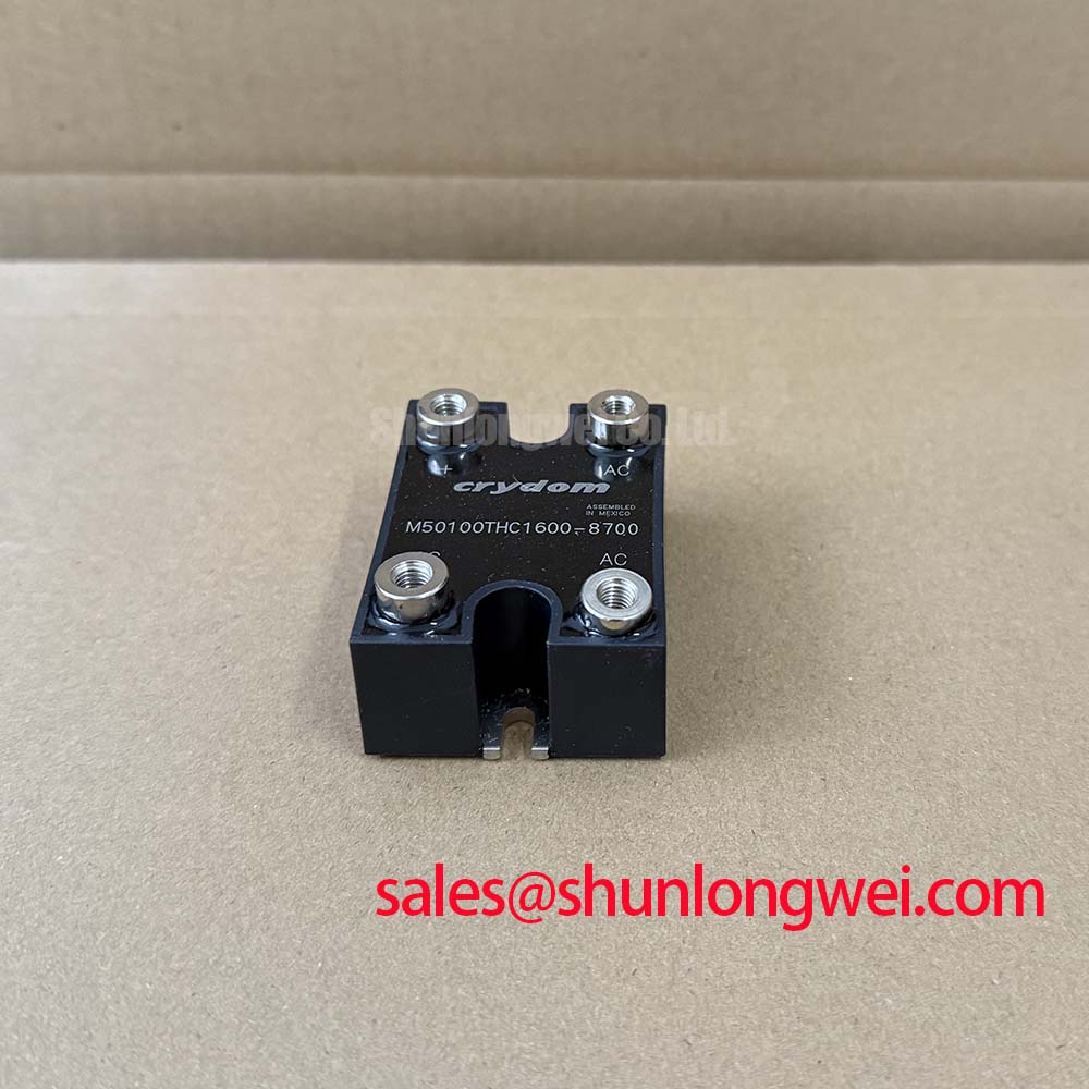
Before reconnecting a removed M50100THC1600-8700, verify its nameplate ratings against the equipment drawing, inspect each power terminal for heat discoloration, and confirm that the insulating interfaces are clean and dry. This SanRex power module is specified at VDRM 1600 V, Io 100 A for three phase full wave rectification, ITSM 1200 A at 60 Hz for one cycle, and Visol 2500 V AC for one minute.
For phase controlled rectification equipment, firing angle directly changes the average DC output and the displacement between source voltage and current. At an angle near zero, a controlled bridge can transfer the largest average DC voltage permitted by the source waveform. As firing is delayed toward 150 degrees, average DC output declines while reactive power demand and source current distortion can become more important system observations. These relationships are topology dependent and must be evaluated from the actual controller timing, transformer arrangement, capacitor bank condition, and measured phase waveforms.
The supplied factory data identifies voltage, current, surge, isolation, temperature, and torque limits, but it does not provide gate trigger current, gate trigger voltage, holding current, latching current, firing-angle transfer curves, or terminal mapping. Where the original circuit is phase controlled, the system integrator should verify the terminal designation and gate-drive requirements from the original equipment documentation before applying trigger pulses. Do not infer a gate terminal arrangement from the module designation alone.
| Official Specification | Value | Integration Relevance |
|---|---|---|
| Repetitive peak off-state voltage | 1600 V | Verify measured blocking peaks remain within the equipment design boundary. |
| Average rectified output current | 100 A | Specified for three phase full wave service. |
| Surge on-state current | 1200 A | Specified at 60 Hz for one cycle only. |
| Isolation breakdown voltage | 2500 V AC, 1 minute | Factory dielectric withstand specification, not a system clearance certification. |
| Operating junction temperature | −40°C to +125°C | Confirm cooling and enclosure conditions support the installed duty. |
| Terminal and mounting torque | 4.7 N·m / 4.7 N·m | Use the stated mechanical installation requirement. |
Fuse coordination is an Engineering Recommendation rather than an official module fuse selection. Compare the semiconductor fuse’s published pre-arcing and clearing I²t values with the protection study for the installed circuit, including available fault energy and conductor impedance. No module I²t value is provided in the available factory parameters, so a numeric fuse coordination table should not be created without the relevant manufacturer data.
For a related component comparison, M505013F should be reviewed only against its own published electrical ratings, package drawing, terminal layout, and thermal conditions. A shared product family or similar current designation does not establish electrical interchangeability.
Field Diagnostics & Commissioning: Minimizing Commutation Turn-Off Voltage Stress in M50100THC1600-8700 Topologies
During commissioning, capture phase voltage, DC bus voltage, load current, and control timing at the same event rather than diagnosing commutation from a single trace. A ringing turn-off waveform can be associated with stray inductance, an unbalanced source, a degraded suppression network, unsuitable trigger timing, or an external freewheel path. It does not establish one isolated cause without correlation to the complete power path.
The published parameters for M50100THC1600-8700 do not state reverse recovery peak current, reverse recovery time, softness factor, switching loss, or dv/dt capability. Those values must not be estimated as factory specifications. Where commutation behavior depends on a companion diode or other external device, designers should obtain that device’s recovery curves and evaluate them at the actual current, junction temperature, and commutation conditions.
Design Consideration: minimize the physical area of the commutation loop where this reduces inductive voltage overshoot, then verify the peak repetitive stress with suitably rated differential voltage measurement. Probe grounding and bandwidth can materially affect observed ringing, so compare the method against a known-good measurement path before modifying hardware.
Inspect terminal hardware for unequal seating, evidence of loosening, corrosion, or conductor strain. Apply the official 4.7 N·m terminal torque only with the equipment isolated and with the terminal stack-up confirmed against its mechanical drawing. ⚠️ Maintenance Note: Monitor terminal contact temperature during normal duty and check that cooling-air passages remain free of dust buildup.
The external insulation test rating of 2500 V AC for one minute supports verification of the module’s stated dielectric withstand characteristic. It does not by itself define the complete assembly’s creepage distance, clearance, pollution degree, cable insulation class, or high-voltage compliance. Those requirements remain system-level Design Considerations.
M50100THC1600-8700 Thermal-Electrical Optimization: Dynamic Voltage Sharing and RC Damping in Practical Tuning
Start thermal work at the mechanical interfaces. The official operating junction temperature range is −40°C to +125°C; it is not a declaration that every mounting arrangement, airflow condition, or load profile will keep the junction within that range. Check heatsink flatness, remove old thermal interface material where maintenance practice requires it, inspect for moisture exposure or condensation, and confirm that both module mounting points are tightened to the specified 4.7 N·m.
When an RC damping network is present in the original equipment, retain its established function during fault finding. Design Consideration: snubber capacitance, resistance, placement, and any series saturable reactor must be selected from measured switching energy, repetitive voltage peaks, component dissipation, and the system’s control sequence. A damping value copied from another converter can alter losses or fail to control a different commutation loop.
In assemblies using series-connected blocking devices, dynamic voltage sharing is determined by the complete network, including static balancing elements, transient suppression, device characteristics, layout, and drive timing where applicable. The 1600 V VDRM rating is an Official Datasheet Specification for this module; it should not be converted into a prescribed series-stack design margin without measured voltage sharing results.
For rectifier-side or complementary power-stage investigation, the PD25016A page provides a separate component reference. Verify its electrical role from the schematic before treating it as a companion device, because a rectifier, freewheel path, clamp, or auxiliary supply path imposes different electrical demands.
Benchtop Waveform Tuning: Mitigating Stress via Non-Repetitive Surge On-State Current on M50100THC1600-8700
The stated 1200 A surge on-state current applies to a 60 Hz, one-cycle event. This is an Official Datasheet Specification for non-repetitive surge endurance under the stated condition, not a continuous current rating, a repeated inrush allowance, or a site-specific fault-clearing guarantee. After a surge event, isolate the equipment and review upstream fuse operation, source condition, load faults, terminal integrity, and thermal interface condition before returning the system to service.
Bench evaluation should begin with controlled low-energy verification of intended blocking and conduction states, followed by waveform review under the equipment’s approved commissioning procedure. Before reverse voltage is reapplied after a surge or abnormal commutation event, verify that the protection path has cleared as intended and that the thermal condition is acceptable for the next test. The available specifications do not provide a junction-temperature recovery curve, so a fixed cooling interval should not be asserted.
For grid-tied static var compensator and thyristor-switched capacitor equipment, this module can be assessed as part of the relevant power conversion or switching subsystem, subject to confirmation of topology, terminal assignment, insulation arrangement, and controller behavior. A capacitor-bank fault, mistimed switching command, or source imbalance requires system-level analysis rather than a module-only diagnosis.
For broader discussion of voltage-class choices in three-phase conversion, see The 1200 V CoolSiC™ MOSFET Advantage in Three. That technical topic concerns a different semiconductor technology and must not be used to substitute specifications for this 1600 V module. Likewise, display-oriented references such as Color Temperature and White Point Calibration in Displays concern optical calibration and have no basis for setting electrical stress limits in a power module.