Content last revised on October 8, 2026
Assembly Integrity and Layout Architecture for MG15N6EK1
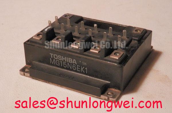
With the unit isolated from all stored energy, begin by checking collector, emitter, and gate terminal identification against the original equipment documentation before reconnecting the MG15N6EK1. A bench diode mode check can help identify an unexpected low resistance collector to emitter path, while a gate to power terminal check should be compared with a known good assembly or the approved incoming inspection baseline. This is a static screening method, not a substitute for dynamic switching validation.
The Toshiba MG15N6EK1 IGBT module is rated at VCES = 1000 V and IC = 15 A DC at the stated 25°C datasheet condition, with a typical VCE(sat) of 2.1 V, typical fall time of 0.35 µs, and collector power dissipation of 80 W under specified datasheet thermal conditions. These are Official Datasheet Specifications and should be checked against the electrical boundaries of the installed inverter before a repair return to service.
| Official Specification | Value |
|---|---|
| Collector emitter voltage, VCES | 1000 V |
| Collector current, IC, DC at the stated 25°C datasheet condition | 15 A |
| Collector emitter saturation voltage, VCE(sat), typical | 2.1 V under specified test conditions |
| Fall time, tf, typical | 0.35 µs under specified test conditions |
| Collector power dissipation, PC | 80 W under specified datasheet thermal conditions |
Before installation, inspect the power terminal surfaces, mounting plane, busbar contact faces, and gate wiring for discoloration, loose hardware, contamination, or evidence of local heating. A connection can show acceptable continuity on a handheld meter and still create a switching problem when current rises. In compact industrial inverter repairs, the busbar path, DC link capacitor placement, gate driver return path, and module terminals must be considered as one current loop.
The 2.1 V typical VCE(sat) value provides a reference point for conduction loss assessment, but it is not a fixed voltage at every load current or temperature. Designers should verify measured collector emitter behavior under the actual gate drive condition, load profile, junction temperature range, and cooling arrangement. A positive temperature coefficient can assist static current sharing in suitably matched parallel IGBT arrangements, but this general behavior does not ensure dynamic sharing. Dynamic balance depends strongly on symmetrical gate wiring, equivalent power loop geometry, matched driver timing, and comparable thermal paths.
Design Consideration: keep the outgoing and return conductors of each switching loop physically close, with equivalent route length where devices are intended to operate in parallel. This reduces unequal parasitic inductance that can otherwise shift switching voltage and current from one device to another. The system engineer should verify peak collector emitter voltage and current distribution with suitable isolated measurement equipment during representative switching tests.
For a compact inverter or high speed CNC spindle drive, inspect whether the DC link capacitor bank is electrically close to the switching bridge rather than only mechanically nearby. Long busbar routes can add loop inductance and make a normal gate command appear unstable at the collector node. If oscillation, uneven heating, or repeated protection events occur, compare the physical conductor routing on each bridge leg before changing gate components.
💡 Bench Tip: Record cold state diode mode and insulation measurements before removal, then compare the replacement assembly under the same meter polarity and ESD controlled handling conditions.
When a repair evaluation requires comparison with another power module, the MG100Q1ZS40 should be reviewed as a separate device with its own ratings, pin arrangement, thermal interface, and switching data. Similar product naming or mechanical appearance alone does not establish interchangeability.
Field Diagnostics and Commissioning for MG15N6EK1 Protection Paths
Commissioning should begin with terminal mapping rather than energization. Identify each power and control terminal from the original equipment documentation, then inspect the gate driver connector, driver return route, DC link polarity, and protective earth arrangement. The system integrator should verify creepage and clearance requirements from the equipment safety design and applicable installation standard, because those distances are determined by operating voltage, contamination conditions, enclosure construction, and local compliance requirements.
The official 1000 V collector emitter voltage rating must not be treated as the expected switching peak in a working inverter. During turn off, stray inductance can add voltage to the DC bus potential. In engineering terms, the peak collector emitter voltage rises with DC bus voltage and with the product of loop inductance and current change rate. This is an Engineering Calculation principle, and the actual margin must be verified on the finished power stage with the intended load, switching frequency, capacitor arrangement, and probe method.
Desaturation protection can provide a useful indication that collector emitter voltage is not collapsing as expected after the gate command has been applied. Its threshold, blanking interval, response time, and coordination with the gate driver must be determined by the driver circuit and system protection architecture. Do not assume a universal short circuit timing capability for this module where no applicable manufacturer short circuit specification has been provided. If a desaturation event occurs, capture the gate signal, collector emitter waveform, DC link behavior, and fault sequence before replacing components.
A staged or soft turn off response is commonly evaluated as a Design Consideration when protection triggers under load. The purpose is to manage the interaction between current interruption and stray inductance, reducing the risk of a sharp collector voltage rise. Its effectiveness depends on the gate driver design, busbar geometry, snubber network, and load condition. The system engineer should validate the waveform rather than relying on a nominal component value copied from another inverter platform.
Mechanical checks remain important during commissioning. Confirm that busbars sit flat on their terminal contact areas, that locking hardware is appropriate to the assembly, and that vibration cannot progressively loosen a current carrying joint. Loose fastening may produce heat, voltage disturbance, or intermittent fault behavior that resembles gate driver failure.
Where the inverter includes a rectifier or an auxiliary power conversion stage, the MG150Q1JS40 can be reviewed as a separate associated power component. Its use in a particular topology must be confirmed from the equipment schematic and its own official specifications.
MG15N6EK1 Circuit Protection and DC Link Layout Control
The 0.35 µs typical fall time indicates that switching transitions can be fast enough for layout quality to materially affect observed waveforms. It does not define a required gate resistor, a permitted loop inductance, or a safe switching frequency for every application. Those values are system determined and require validation with the installed driver, load, DC bus, thermal arrangement, and electromagnetic environment.
Design Consideration: position the local DC link energy source so the commutation loop is compact, and route positive and negative conductors as a closely coupled pair. The objective is to minimize parasitic loop inductance and suppress turn off inductive overshoot. A planar or closely coupled busbar arrangement can help where the mechanical design permits it, but its result should be verified by measuring the switching waveform at the module terminals with an appropriate probing method.
A snubber network should only be selected after the actual ringing frequency, peak voltage, energy source, and switching operating point have been examined. A capacitor that appears to reduce ringing at low load can alter losses or resonance at another load point. Engineers should first confirm the DC link capacitor condition, terminal contact integrity, gate driver stability, and measurement technique before attributing voltage spikes to the module itself.
For incoming inspection, compare collector emitter behavior in diode mode with the same probe polarity across units from the same approved repair workflow. An unexpected result can indicate a damaged power path, an incorrect terminal interpretation, or a test condition difference. It does not on its own identify the origin of an equipment failure. Gate to power terminal measurements should also be conducted only after the module has been electrically isolated from surrounding driver circuitry.
The gate circuit deserves the same physical discipline as the power circuit. Keep the gate command and its return path paired, avoid sharing a noisy high current return path with sensitive drive references, and verify dead time under actual operating conditions. Negative gate bias, if present in the original drive, should be retained only according to the established driver design and validated for common mode disturbance behavior. The MG15N6EK1 official data listed here does not specify a required negative gate voltage.
For broader discussion of industrial drive switching efficiency and waveform evaluation, see Unlocking Efficiency in Industrial Drives. Material relating to optical anti reflective coatings, such as this reference on anti reflective coating, applies to display optics rather than the electrical characteristics of this IGBT module.
MG15N6EK1 Thermal Electrical Operating Margin Evaluation
The 80 W collector power dissipation rating is an Official Datasheet Specification, but system dissipation depends on conduction loss, switching loss, duty cycle, current waveform, gate drive behavior, heatsink condition, thermal interface quality, and ambient environment. The typical 2.1 V VCE(sat) value can support a first conduction loss estimate, yet an installed inverter should be assessed using measured operating current and temperature behavior rather than typical data alone.
Before reassembly, inspect the heatsink mounting surface for residue, flatness concerns, and marks that could prevent uniform thermal contact. Apply the thermal interface material in accordance with the original equipment procedure or the relevant material supplier guidance. The module mounting arrangement, screw specification, tightening sequence, and torque must be verified from the equipment documentation because no mounting torque or package dimensions are included in the official parameters provided for MG15N6EK1.
In high speed CNC spindle drives, repeated acceleration and deceleration can create varying electrical and thermal demand. The system integrator should monitor heatsink temperature, output current, DC link ripple behavior, and protection events across the real duty cycle. If thermal stress is suspected, compare measured waveforms and temperature trends before adjusting switching settings or substituting parts.
Altitude, neutron related single event burnout, FIT rates, service life, insulation reliability, and compliance status cannot be quantified from the supplied MG15N6EK1 specifications. Design Consideration: where equipment will operate at elevated altitude or in an unusual environment, the responsible system designer should assess voltage derating, cooling capability, enclosure conditions, and applicable safety requirements using verified system level documentation. No specific failure rate or operating life should be inferred from the module ratings stated above.
For maintenance decisions, retain a record of the original DC bus operating voltage, protective trip history, gate driver waveform, cold state terminal checks, and heatsink condition. This evidence gives repair engineers a more reliable basis for evaluating whether the MG15N6EK1 remains within the electrical and thermal boundaries established by the host equipment.