Content last revised on October 3, 2026
MG30G6EL2 Circuit Protection & Reliability: Calibrating Thermal Paste Degradation Prevention and Mounting Practice
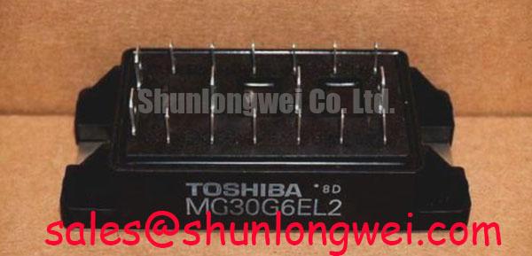
Verify the nameplate against MG30G6EL2, inspect the Toshiba module body for housing damage, and confirm the cold-state resistance of each accessible power path before reconnecting the inverter or robot-axis drive.
| Parameter | Official Specification | Engineering Use |
|---|---|---|
| Manufacturer | Toshiba | Confirm the original equipment documentation before replacement |
| Model | MG30G6EL2 | Use the complete ordering code during service procurement |
| Rated voltage | 600.0 V | Compare with the measured DC-link and switching environment |
| Rated current | 30.0 A | Evaluate alongside temperature, switching frequency, duty cycle, and cooling |
| Package | Toshiba Module | Check mechanical fit, terminal arrangement, insulation, and heatsink interface |
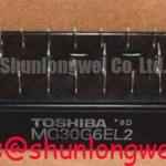
The MG30G6EL2 is a Toshiba IGBT module specified at 600.0 V and 30.0 A, supplied in a Toshiba module package. These are official product specifications, not a complete system operating limit. Actual junction temperature and usable current depend on the switching waveform, thermal path, ambient conditions, gate-drive behavior, and the equipment manufacturer’s application data.
During field replacement, clean the heatsink contact area and remove old, hardened thermal interface material before positioning the module. The contact surfaces should be free of metal fragments, oxidized paste, and raised contamination. A thermal interface layer should be continuous and thin enough to fill microscopic surface irregularities without creating a thick insulating film. The exact material, application thickness, and mounting torque should be selected from the module documentation and the heatsink supplier’s instructions rather than assumed from a general-purpose compound.
Uniform clamping is important because a distorted baseplate or uneven screw sequence can create local thermal resistance. Tighten the mounting hardware gradually in a crosswise sequence where the mechanical design permits it, allowing the module base to settle evenly against the heatsink. Designers should verify the final torque, screw grade, washer arrangement, and thread condition against the applicable mechanical drawing. The module should not be forced into alignment by the power terminals.
Thermal degradation is often gradual. During preventive maintenance, inspect the heatsink for blocked airflow, dust accumulation, loose fan guards, and signs of compound migration. Compare case or heatsink temperature with an earlier known-good operating condition under a similar load. A rising temperature difference does not identify one single failure mechanism; it may also reflect increased switching loss, altered load duty, poor airflow, terminal resistance, or a change in the control sequence.
For light industrial automation and multi-joint robotic articulators, compatibility review should include the drive’s DC-link voltage, braking conditions, pulse current, regenerative energy, and enclosure airflow. A 600 V rating alone does not confirm suitability for every 600 V-class inverter. The service engineer should verify switching conditions and protection margins using the original drive schematic and the Toshiba technical documentation.
Maintenance Note: De-energize and discharge the drive before touching the module, and verify the cooling path and terminal tightness during every scheduled inspection.
Assembly Integrity & Layout Architecture: Implementing Multi-Module Parallel Current Sharing for MG30G6EL2
Parallel use requires system-level validation and should not be inferred from the 30.0 A rating of one device. When designers evaluate multiple modules for a shared-current arrangement, the electrical paths must be symmetrical in resistance and inductance. Power bus length, copper geometry, terminal pressure, emitter return routing, and gate-loop placement all affect how current divides during switching.
Static current sharing may benefit when the relevant conduction voltage has a positive temperature coefficient over the intended operating region, but this behavior must be confirmed from the manufacturer’s electrical characteristics for the exact device and temperature range. It should not be treated as a guaranteed substitute for matched layout and thermal design. Measure current in each branch during controlled load tests, then repeat the test at representative temperature and switching conditions.
Gate wiring deserves the same attention as the collector and emitter paths. Keep the gate-drive connections physically consistent between parallel devices, avoid routing one gate loop beside a high-current commutation path, and confirm that each driver output sees the expected gate-emitter behavior. If a shared driver is used, the system designer should verify the driver’s source and sink capability, protection strategy, and propagation balance. If separate channels are used, timing and reference integrity require measurement rather than visual inspection alone.
The freewheeling diode path also influences current balance and electromagnetic behavior. Reverse-recovery charge, commutation inductance, DC-link impedance, and gate resistance can combine to produce overshoot or ringing. A snubber may reduce unwanted voltage oscillation, but its component values and placement are system-dependent. Engineers should select and validate the network while observing collector-emitter voltage, gate-emitter voltage, diode current, and radiated or conducted interference during switching tests.
For a robotic axis drive, inspect the complete commutation loop from the DC-link capacitor to the high-current terminals and back through the return path. Long cable runs to the motor can add another source of transient stress, especially where braking or rapid deceleration causes regenerative energy. The inverter designer should verify peak voltage against the device’s rated boundary and confirm that the control system does not produce an abnormal pulse pattern during acceleration, reversal, or emergency stop.
When a larger current class is required, the MG100Q1ZS40 can be reviewed as a separate Toshiba product for objective package, rating, and application comparison. It should not be treated as a direct replacement without checking the circuit topology, mounting pattern, gate characteristics, protection settings, and thermal design.
Preventing Spurious Faults: Transient Thermal Impedance Guidelines for MG30G6EL2
Short overload pulses can produce a junction temperature rise before the heatsink temperature changes visibly. A transient thermal impedance model represents this behavior through several thermal time constants, but the correct resistance and time-constant values must come from the relevant Toshiba data. Without those curves, a numerical junction-temperature prediction would be speculative.
For engineering evaluation, capture the actual collector-emitter voltage, collector current, pulse duration, repetition pattern, and case temperature. Use the recorded waveform with the manufacturer’s transient thermal impedance information to estimate the junction response. The calculation should include the real pulse sequence rather than only the average current, because repeated overloads can accumulate heat when the cooling interval is short.
A practical investigation begins with the fault log and the operating sequence. Determine whether the event occurs during motor acceleration, deceleration, axis holding, power-up, or a protective stop. Then compare the gate waveform and power waveform with a known-good channel. A gate disturbance may indicate common-emitter inductance, driver supply instability, excessive loop coupling, or an incorrect dead-time relationship; the oscilloscope record should establish which condition is present.
Thermal interface aging should be considered alongside electrical causes. A module may show acceptable idle temperature while developing excessive thermal rise during repeated motion cycles. Check the heatsink temperature at a consistent measurement location, inspect fan performance, and compare the measured thermal trend with the original maintenance record. Do not assign a fixed lifetime or failure probability without a qualified reliability source and the actual operating profile.
Clearance and creepage around the module, busbar, and gate-drive board should follow the applicable equipment standard and the original insulation design. Keep conductive debris, condensation, and loose cable strands away from the power terminals. In cold or humid industrial environments, allow the enclosure and module surfaces to reach a stable condition before energizing if condensation is possible. The equipment designer remains responsible for validating insulation performance under the intended environmental conditions.
Engineers reviewing broader inverter and energy-conversion service conditions may also consult the industrial applications reference for general context. It does not replace the Toshiba data for MG30G6EL2 or establish a guaranteed operating profile for a particular robot drive.
MG30G6EL2 Circuit Protection & Reliability: Calibrating Short-Circuit Protection and Controlled Turn-Off
Short-circuit protection must be coordinated with the actual driver, current sensor, desaturation or overcurrent circuit, wiring inductance, and the module’s permitted short-circuit behavior. A generic response time cannot be assigned to MG30G6EL2 without the manufacturer’s short-circuit safe-operating-area information and the complete gate-drive design. The protection engineer should confirm the available detection interval against the specified device data before releasing the inverter for production use.
During commissioning, test the protection circuit at a controlled energy level and with appropriate isolation and emergency controls. Observe the gate-emitter voltage, collector-emitter voltage, fault signal, driver supply, and DC-link behavior together. The objective is to verify that the fault is detected consistently and that the turn-off transition does not create an excessive inductive voltage spike.
A two-stage turn-off strategy can be considered when the driver and module data support it. The first stage limits the immediate gate-drive action, while a controlled final turn-off reduces the risk of an abrupt current change. The exact gate resistance, timing, voltage levels, and clamp behavior must be determined by the system designer from measured waveforms and the applicable Toshiba specifications. These values should not be copied from another IGBT family.
After a protective trip, inspect the event history before replacing the module. Check whether the fault was associated with a motor cable issue, a failed diode path, an unstable gate supply, an incorrect dead-time setting, a DC-link transient, or a mechanical load jam. A repeated fault code is evidence for a measurement plan, not proof of one failed component. Compare the affected phase with an unaffected phase wherever the circuit allows safe testing.
For procurement and maintenance records, retain the full MG30G6EL2 ordering code, Toshiba manufacturer identification, rated 600.0 V voltage, rated 30.0 A current, package description, installation date, and the measured operating conditions. This information helps the next service engineer distinguish a device-rating issue from a gate-drive, cooling, wiring, or load-related problem.