
Content last revised on October 5, 2026
MG75J1ZS50 Assembly Integrity and Current Sharing
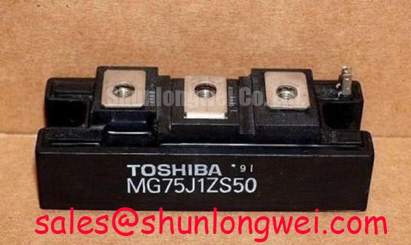
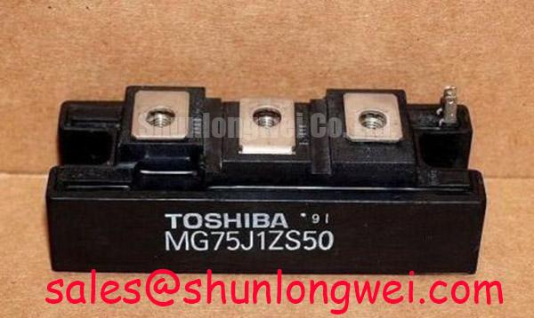
Check the terminal markings and the original equipment schematic before putting a meter across a disconnected MG75J1ZS50. Toshiba identifies this part as a module with a 600 V voltage rating and a 75 A current rating (Official Specification). Those ratings establish the first limits for an incoming inspection, but they do not establish the terminal arrangement, an acceptable diode reading, or a safe operating DC bus on their own.
Begin the bench record with photographs of the case, terminals, mounting face, and equipment wiring before removing the old unit. Match each power and control connection to the original schematic rather than inferring polarity from the positions of the terminals. With the module disconnected, compare cold resistance readings across corresponding paths against an established, serviceable reference, using the same meter range and lead orientation. A differing reading is a reason to investigate the circuit path and test setup, not a diagnosis by itself.
If the documented terminal arrangement includes a diode path, use the meter’s diode function in both directions and record the displayed forward reading and reverse indication. Probe contact, connected circuitry, and meter test current can affect the result. Do not assign a universal pass voltage to MG75J1ZS50 without a specified test condition. 💡 Bench Tip: Keep the gate terminals protected during handling and compare cold readings only after the module is isolated from the equipment circuit.
For an assembly that parallels switching devices, current sharing is a system-level Design Consideration. A positive temperature coefficient of saturation voltage can support static sharing under applicable operating conditions, but it must not be assumed for this part without the relevant Toshiba characteristic data. Gate-loop symmetry matters separately: unequal wiring impedance can produce different switching behavior even when cold meter readings appear alike. Designers should compare gate connections, busbar paths, and switching waveforms before approving a parallel arrangement.
When evaluating MG75H6EL1 alongside the MG75J1ZS50, treat it as a comparison candidate, not a confirmed direct replacement. The decision depends on the documented topology, terminal assignment, mounting interface, gate requirements, and thermal limits of the actual equipment.
MG75J1ZS50 DC-Bus Headroom and Drive Interlocks
The 600 V rating (Official Specification) is a device voltage boundary, not a recommended DC-bus setting. For a variable frequency AC motor drive under repair, measure or obtain the actual bus operating range, then capture collector-to-emitter voltage during representative switching and braking conditions. The system designer should verify that transient peaks remain within the applicable device limits. Reducing parasitic loop inductance is a Design Consideration for controlling turn-off overshoot; the required layout and operating margin must be established by measurement in the finished drive.
Do not calculate a single-event burnout rate, altitude derating, or service-life prediction from the voltage rating alone. Such figures require device-specific evidence and stated environmental and operating assumptions. If an installation has unusual altitude or exposure requirements, request the applicable reliability data and assess the complete drive rather than assigning an unsupported failure rate to this module.
Check the drive schematic before discussing complementary gate timing: the supplied ratings do not identify the internal switching topology of MG75J1ZS50. Where the equipment uses complementary switches, dead time and hardware interlocks are Design Considerations for preventing simultaneous conduction. Verify gate signals at the module connections during controlled testing; controller commands alone may not reveal propagation delay or wiring differences. Information on direct torque control can help place a motor-drive control method in context, but it does not set this module’s switching limits.
Tracing the wider power path can also prevent a module-level fault from being confused with a DC-link or upstream-stage fault. The MG100Q1ZS40 is another module to evaluate where an equipment schematic identifies a relevant surrounding stage; its function and compatibility must be confirmed from that schematic and its own documentation.
MG75J1ZS50 Thermal Contact and Mounting Checks
Inspect the heatsink contact area before installing the module. Remove old interface material using a method compatible with the surfaces, then check for debris, raised edges, and visible damage that could prevent even seating. An uneven mounting face can increase thermal resistance despite sound electrical connections. Record the condition of both surfaces so that a later temperature discrepancy can be assessed against the installation work.
A thin, continuous thermal interface layer and a gradual, alternating tightening sequence are Design Considerations, not published MG75J1ZS50 thickness or torque specifications in the information available here. Select the interface material and mounting procedure from the applicable Toshiba and equipment documentation. Avoid compensating for a visibly distorted surface by adding more compound; the mounting geometry needs assessment first.
During a controlled return to service, compare module case or heatsink temperatures at repeatable operating conditions, while checking current and cooling airflow. A temperature difference may reflect contact pressure, interface coverage, loading, or a cooling-system issue. It does not, by itself, identify an internal defect. In a heavy-duty variable frequency drive compatibility assessment, the mechanical envelope and cooling arrangement deserve the same attention as the 75 A current rating (Official Specification).
MG75J1ZS50 Gate Protection and Miller Clamp Limits
Check the installed gate-driver circuit before changing its off-state behavior. Collector voltage transitions can couple into a gate circuit through device capacitance, making unintended turn-on a concern in some switching arrangements. A low-impedance off-state path or an active Miller clamp is a possible system Design Consideration, but the available MG75J1ZS50 ratings do not establish that either measure is required or define a suitable negative gate bias.
If the drive already has a clamp or negative-bias supply, inspect its connections and capture gate-to-emitter waveforms at the module during controlled switching. Compare the observed off-state voltage with the driver and device documentation, and check for differences between commanded states and measured terminal behavior. Gate-driver selection and isolation are circuit-level tasks; TI’s isolated gate-driver overview provides context, not an approval of a particular driver for this module.
For fault tracing, separate the evidence from the suspected cause: record bus voltage, gate waveform, switching-node waveform, load condition, and heatsink condition under the same test conditions. The IGBT Design & Integration reference covers the gate-drive, thermal, and circuit-topology relationships relevant to that review. Final clamp behavior and protection timing should be verified in the equipment circuit against its documented limits.