

Content last revised on September 10, 2026
MUBW15-12A7 Repair Assessment and QA Checks
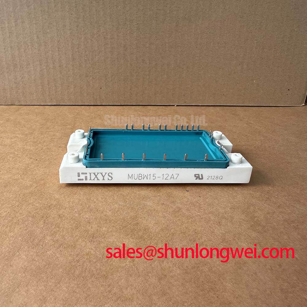
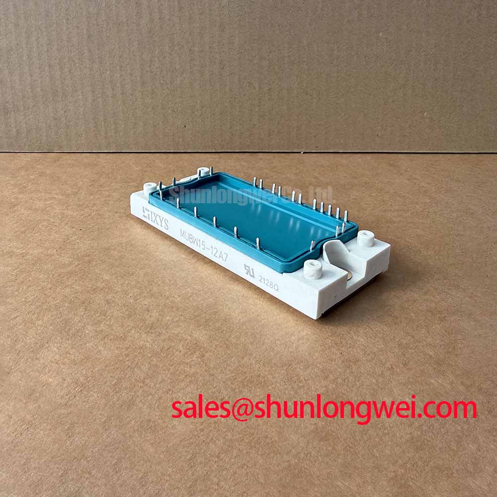
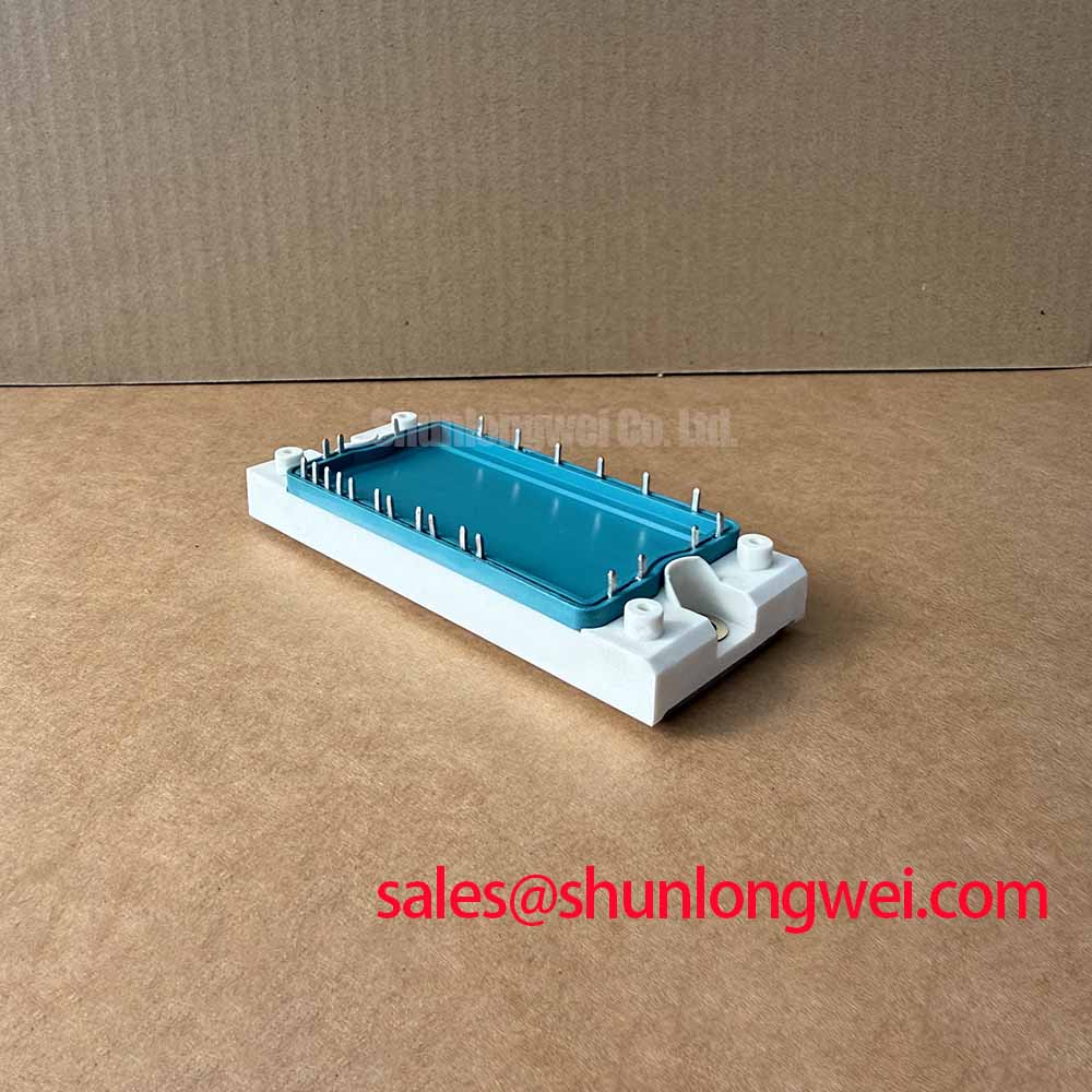
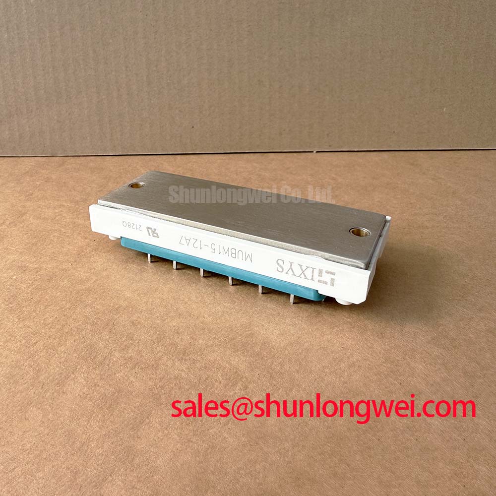
Before connecting a replacement module, verify each rectifier path with a cold digital multimeter diode test and compare the observed polarity with the drive’s original terminal map. The MUBW15-12A7 from IXYS is a power integrated module that combines a three phase input rectifier, a brake chopper with IGBT and fast recovery diode, and a six pack IGBT inverter stage for compact motor drive power conversion.
The official electrical limits establish the starting point for any repair assessment. The input rectifier is rated at VRRM = 1600 V and IFAV = 15 A under the specified datasheet conditions. The brake chopper and inverter IGBTs are each rated at VCES = 1200 V and IC = 15 A under the specified datasheet conditions. The module carries an official isolation specification of VISOL = 2500 VAC for 1 minute. These are Official Datasheet Specifications and should be checked against the voltage class and connection architecture of the existing variable frequency drive.
| Functional block | Official specification | Incoming QA check |
|---|---|---|
| Input rectifier | Three phase diode bridge, VRRM 1600 V, IFAV 15 A | Cold diode mode comparison across each expected path |
| Brake chopper | IGBT and fast recovery diode, VCES 1200 V, IC 15 A | Static gate threshold verification at IC 0.5 mA |
| Inverter | Six pack IGBT topology, VCES 1200 V, IC 15 A | ICES below 250 µA at 1200 V and 25°C |
| Isolation | Module isolation, VISOL 2500 VAC for 1 minute | Controlled hi-pot test using the applicable test method |
MUBW15-12A7 Operational Boundaries: Evaluating Dynamic Power Loss Dissipation and Multi R Limits
Start thermal evaluation from the actual drive duty cycle, not from the continuous current label alone. The 15 A collector current rating is an Official Datasheet Specification, while junction temperature rise during acceleration, regenerative braking, and repetitive overload is determined by switching conditions, conduction loss, heatsink behavior, airflow, and the thermal path established during mounting. The provided structured specification does not define a thermal resistance network, transient thermal impedance curve, maximum junction temperature, or overload waveform. Those values must therefore be taken from the applicable manufacturer documentation for the installed assembly before a multi RC transient thermal calculation is attempted.
A multi RC thermal model is useful because short power pulses and prolonged high load intervals do not produce the same junction response. Engineering Calculation requires verified thermal resistance and time constant data, together with measured or calculated device loss. Without those inputs, a numerical peak junction margin would be speculative. During service work, a more reliable first action is to inspect the heatsink contact area, confirm flat seating, review cooling path obstruction, and compare load current, DC link behavior, and heatsink temperature with the known operating condition of the machine.
For a heavy duty variable frequency AC motor drive, the rectifier, braking path, and inverter should be assessed as connected functions. A brake event can raise DC link energy while the inverter is simultaneously handling motor current. The braking resistor circuit, chopper control signal, and DC link capacitor condition can each influence the electrical and thermal loading seen by the module. A failed braking path should not automatically be attributed to the chopper IGBT. Verify the resistor, wiring, command logic, DC link measurement path, and gate drive behavior before assigning the fault to the power module.
The specified input diode test reference is 0.65 V to 0.80 V at 1 mA. This QA Bench Measurement Method is suitable for cold comparison of expected rectifier junctions, provided that the test is made with the module removed or electrically isolated from parallel drive circuitry. A substantially inconsistent result can justify further investigation, but it does not establish the condition of the dynamic inverter stage. Gate threshold testing for the brake chopper at IC = 0.5 mA should be performed only with suitable controlled test equipment and correct terminal identification.
💡 Bench Tip: Discharge the DC link, use ESD controlled handling, and record cold readings before reconnecting gate drive or motor cables.
Design Consideration: an MOV coordinated with the DC link protection network can help limit external surge exposure when its voltage rating, energy capability, placement, fuse coordination, and thermal environment have been validated for the complete drive. The MOV is not a substitute for controlling inductive switching overshoot at the module terminals. For equipment with a bidirectional DC DC battery interface, engineers should also evaluate charge and discharge duty as a thermal cycling condition across the entire converter, because the module’s actual stress depends on the system power path and control operation.
Where a repair evaluation requires a related integrated module reference, the P950A should be treated as a separate part for documented comparison of circuit arrangement, pin assignment, ratings, mounting interface, and gate drive compatibility. Matching headline voltage and current values alone does not demonstrate interchangeability.
Transient Dynamics & Electrical Design: High Frequency Commutation Loop Inductance on MUBW15-12A7
The inverter stage should be examined with the DC link capacitor, bus conductors, module terminals, and gate return path considered as one switching loop. During turn off, the voltage at the switching device rises above the DC link by an inductive term related to loop inductance and the rate of current change. This is the familiar relationship in which peak voltage combines DC link voltage with Lσ multiplied by di/dt. It is an Engineering Principle, not a confirmed switching limit for this module, because the supplied official data does not state switching energy, allowable transient overshoot, gate resistance, or switching frequency.
Design Consideration: minimize the physical area enclosed by the positive and negative DC link paths to suppress inductive overshoot during commutation. Closely coupled conductor geometry, short routes between the local DC link capacitor and power terminals, and symmetric current paths are commonly evaluated. The system engineer should verify peak collector emitter voltage with correctly rated differential measurement equipment during representative switching tests, then compare the observed result with the official 1200 V VCES rating and the complete design margin policy.
A snubber network requires the same discipline. Its capacitor value, voltage rating, resistor selection, physical placement, and loss capability depend on measured ringing frequency, stored inductive energy, DC link condition, and switching pattern. The available product data does not prescribe a snubber value. An Engineering Recommendation is to characterize the existing waveform first, including the probe arrangement, because a long measurement ground lead can introduce misleading ringing into the observed trace.
Common mode ground movement can disturb a gate drive reference, particularly when high current return paths share impedance with gate control paths. The supplied specifications do not define a mandatory negative gate bias for MUBW15-12A7. Designers should verify the original driver documentation, permitted gate voltage range, and turn off behavior before changing bias conditions. Adding an unverified negative bias or changing damping components can alter both switching loss and transient response.
The 2500 VAC for 1 minute module isolation specification is an Official Datasheet Specification for the stated test condition. It should not be interpreted as a blanket statement about enclosure insulation, installation clearance, cable insulation, or complete drive safety compliance. During incoming QA, a controlled hi-pot check may be used to assess isolation under the applicable test method. Use test equipment procedures that protect personnel and avoid applying an unsuitable test to connected control electronics.
When evaluating current feedback stability in the surrounding drive, the sensor placement and signal return deserve inspection. Industrial current measurement may use several sensing methods; background on magnetoresistive sensing can be reviewed through GMR and TMR sensor principles. That reference describes sensor technology rather than a confirmed feature of this IXYS module. The original drive schematic remains the authority for its feedback implementation.
Preventing Spurious Faults: Thermal Interface Material Thickness Uniformity Guidelines for MUBW15-12A7
Intermittent overtemperature alarms and unequal phase behavior can begin at the mechanical interface, even when cold semiconductor checks appear consistent. Clean the heatsink contact surface and module base contact area using a process compatible with the equipment’s service requirements. Look for dried compound, particles, scoring, corrosion, uneven witness marks, or evidence that the module was not seated uniformly. These observations do not prove a semiconductor fault, but they can identify a thermal transfer issue that deserves correction before powered testing.
Design Consideration: use a thin, continuous thermal interface layer appropriate for the surface condition and manufacturer installation guidance. In general industry practice, a controlled thin application in the range of 50 µm to 80 µm is often used as a starting process target where the mounting system is designed for thermal grease. This is not an IXYS factory thickness requirement for the part. The required material, thickness, and application method must be verified against the original equipment documentation and the actual flatness of the heatsink and module base.
Apply mounting hardware in a cross pattern and build clamp load gradually so the baseplate settles without being pulled down from one side. The official parameter set supplied here does not specify screw size or mounting torque. Do not assign an assumed torque value to this module. The drive manufacturer’s service documentation or the applicable IXYS mechanical drawing should determine fastener type, torque, washer use, tightening sequence, and any insulation hardware.
After installation, inspect terminal hardware separately from base mounting hardware. High resistance at a power terminal can create localized heating and unstable waveform behavior. Verify conductor preparation, terminal seating, fastening method, and torque according to the drive documentation. Keep high current conductors away from sensitive control routes where practical, while maintaining the original creepage and clearance arrangement. Layout dimensions must be determined by the system voltage, pollution environment, enclosure construction, and applicable equipment standard.
A current limited initial power up helps isolate faults without immediately subjecting the replacement module to full machine energy. Observe whether the rectifier establishes the expected DC link, whether a gate drive fault is present, and whether phase outputs remain balanced under the manufacturer approved test procedure. If abnormal current is observed, disconnect power and return to static verification rather than repeatedly resetting the drive. The inverter leakage criterion of ICES below 250 µA at 1200 V and 25°C is an Official Datasheet Specification and requires a suitable controlled high voltage test method. A handheld meter cannot confirm that condition.
For teams assessing longer term technology choices beyond an immediate repair, Wide Bandgap Revolution provides technical context on GaN and SiC device design considerations. It does not change the specified silicon IGBT ratings or interface requirements of the MUBW15-12A7.
MUBW15-12A7 Operational Boundaries: Evaluating Kelvin Emitter Connection Limits
Do not assume that every power module provides a separate Kelvin emitter terminal. The supplied official parameter set identifies the functional power stages and electrical ratings, but it does not provide a terminal drawing or confirm a dedicated auxiliary emitter connection. Before altering a gate return, consult the correct module outline, terminal designation, and original drive schematic. Connecting a driver return to an unverified terminal can create an immediate control malfunction or damage the driver circuit.
Where the original circuit does provide an auxiliary emitter or separate gate reference, Design Consideration is to keep the gate driver return distinct from the main high current emitter path as intended by the module and gate driver documentation. Shared power return impedance can convert rapid current changes into gate reference movement. That movement may appear as unwanted gate voltage, ringing, missed desaturation detection, or nuisance protection response. An oscilloscope measurement referenced safely to the actual driver return can help determine whether the observed issue is related to gate loop behavior, rather than assuming the IGBT itself is defective.
For the six pack inverter, identify each gate and return path one phase at a time, then compare the mapping with the drive control board connector. Record continuity and diode mode observations in a repeatable format. The low side and high side drive references are not interchangeable. The system integrator should verify isolation barriers, driver supply arrangement, dead time control, and protection inputs from the original documentation before applying an external gate test.
The brake chopper gate path requires the same caution. Its static threshold verification at IC = 0.5 mA is an Official QA Bench Measurement Method, not a recommendation for a live drive test. In circuit waveforms must be assessed with the intended controller, DC link condition, load condition, and protection sequence. A waveform irregularity may indicate gate loop coupling, driver supply instability, current sensing behavior, motor cable effects, or a control board fault. Verify each path against the known schematic and a controlled reference measurement before replacing additional parts.