
Content last revised on September 10, 2026
P950A Operational Boundaries: Evaluating High Frequency Common Mode Bearing Current Limits
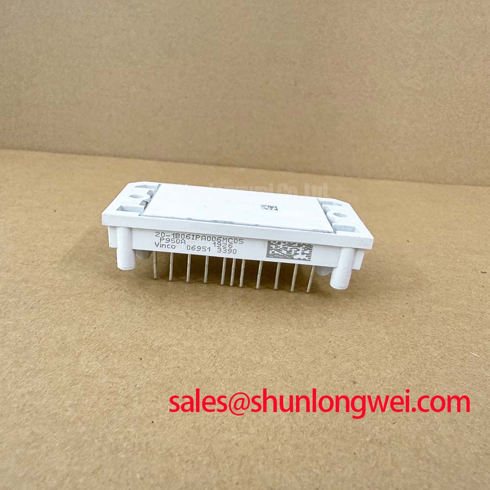
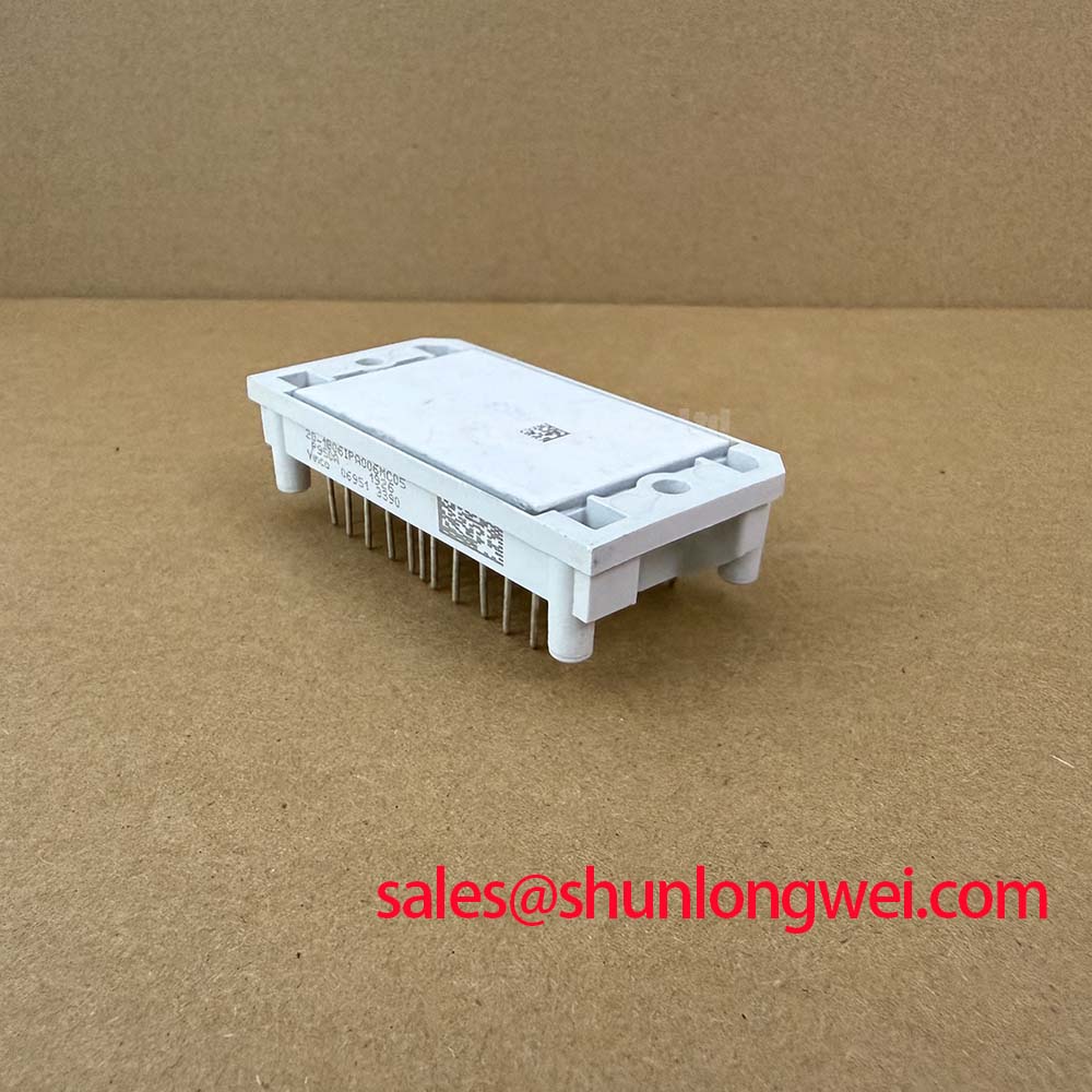
| Manufacturer | Vinco |
|---|---|
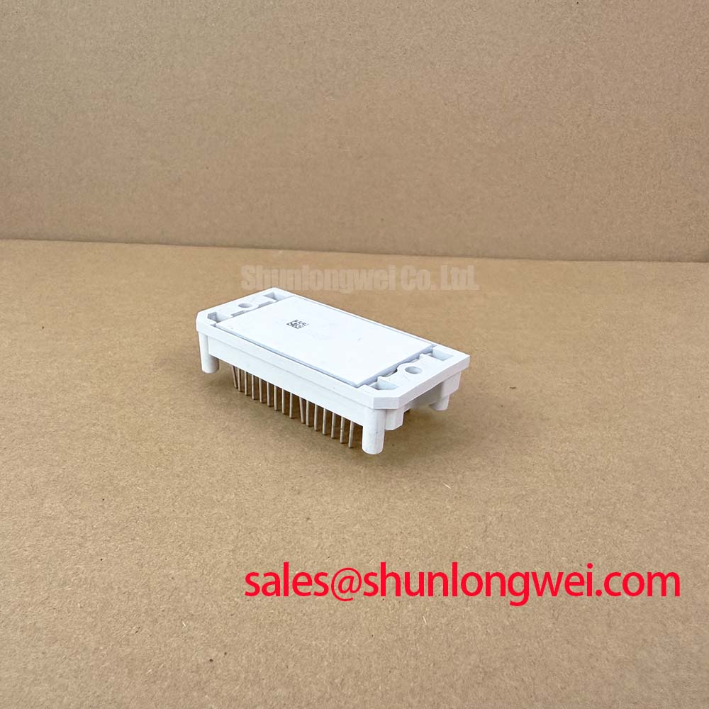
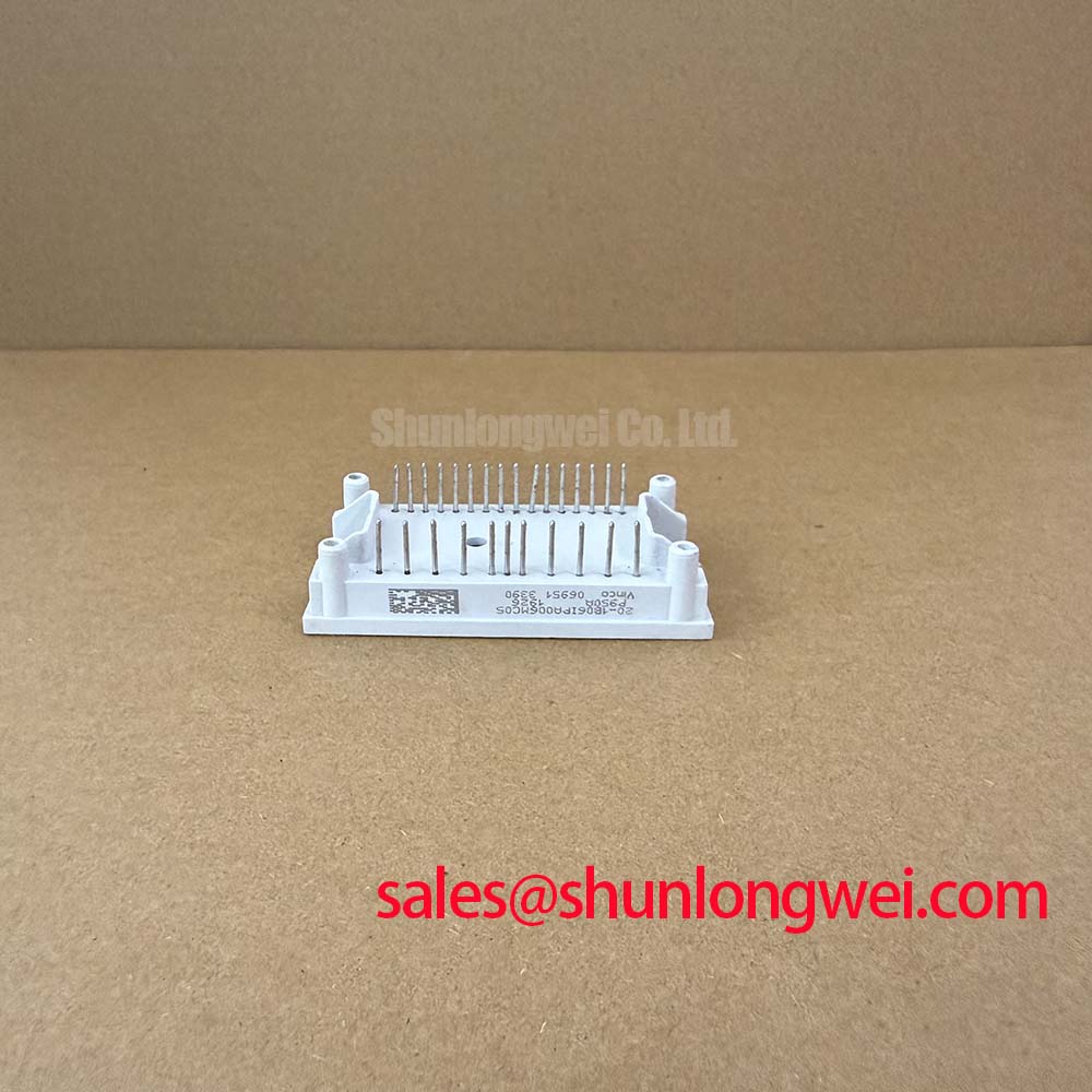
| Product Model | P950A |
| Product Category | IGBT Module |
| Collector Emitter Voltage | 1200V Official Datasheet Specification |
| Gate Emitter Threshold Voltage | 5.8V typical Official Datasheet Specification |
| Junction to Case Thermal Resistance | 0.04°C/W Official Datasheet Specification |
| Integrated Temperature Sensor | NTC included Official Datasheet Specification |
Probe the motor output terminals and DC link with properly rated differential probes while the servo drive operates through controlled acceleration and deceleration, then compare the waveform at the inverter output with the waveform at the motor end of the cable. A steep edge that looks clean at the drive but shows ringing or a higher peak at the motor can indicate transmission line effects in a long motor lead.
The P950A Vinco IGBT module has a 1200V collector emitter rating as an Official Datasheet Specification. That rating is a device boundary, not a permitted operating spike target. In high dynamics CNC and robotics servo systems, reflected-wave behaviour can increase the voltage observed at remote motor terminals. Under severe cable impedance mismatch conditions, terminal peaks can approach twice the DC link voltage. This is a Design Consideration for the complete inverter, motor cable, grounding arrangement, and output filter network rather than an official P950A switching guarantee.
When a drive reports motor insulation alarms, bearing problems, unexplained encoder interference, or repeated overvoltage events after a motor cable change, inspect the practical electrical path first. Confirm shield termination at both ends where the machine grounding concept permits it, inspect cable glands for interrupted shield continuity, and look for output conductors routed beside low-level encoder or feedback wiring. A poor return path can change common-mode current distribution and make a previously stable drive behave differently after field rewiring.
Design Consideration: an output choke or dv/dt filter can reduce edge severity at the motor when measured waveforms show reflected peaks or excessive ringing. Filter selection must be determined from the actual DC link level, cable characteristics, motor insulation capability, switching behaviour, current demand, and servo control requirements. Verify peak voltage margins under representative switching tests rather than selecting a filter from motor cable length alone.
The P950A thermal path also deserves attention during this check. Its 0.04°C/W junction to case thermal resistance is an Official Datasheet Specification, but the finished temperature rise depends on the mounting interface, heatsink condition, airflow, switching losses, current waveform, and control strategy. The integrated NTC gives the drive controller a local temperature input, yet a rising temperature trend should lead to inspection of the cooling path and operating waveform rather than being treated as proof of one isolated failure mechanism.
For comparison work, the BSM22GD120D can be reviewed as a separate IGBT module reference. Package geometry, terminal arrangement, gate-drive requirements, current ratings, thermal arrangement, and protection implementation must be assessed at system level before any replacement decision is made.
P950A Operational Boundaries: Evaluating Dynamic Braking Chopper Operation Limits
Measure DC link behaviour during a controlled deceleration command and observe whether the braking resistor circuit is being enabled at the point where regenerative energy returns from the motor. If the DC link rises while the resistor remains inactive, inspect the braking control signal, chopper gate-drive supply, interlock path, resistor wiring, and resistor thermal protection before attributing the event to the inverter power module.
High dynamics servo axes repeatedly return kinetic energy to the DC link during rapid stopping, direction changes, and vertical-load control. The P950A may operate within an inverter power stage, while braking energy may be handled by a separate internal or external chopper arrangement. Do not assume that the P950A itself contains a braking transistor or a braking resistor connection. Trace the installed drive schematic and terminal allocation to establish where the regenerative-energy path is actually controlled.
Engineering Recommendation: size the braking transistor and ballast resistor from the measured or calculated regenerative energy profile, the deceleration duty cycle, the available DC link energy storage, ambient cooling, and the resistor manufacturer’s pulse capability. The resistor must be treated as a thermal component, not only as an electrical resistance value. Discolouration, cracked cement bodies, loose terminals, damaged insulation, and heat-affected nearby wiring are practical signs that the braking assembly needs closer examination.
Gate timing between complementary switches is equally important. Dead time prevents simultaneous conduction within a switching leg, but excess dead time can alter current transfer and affect control performance. The required non-overlap interval is system-determined by the selected gate driver, device switching response, operating current, temperature, layout inductance, and measured switching waveform. The general principle of non-overlap gate control is described in Dead-Time Insertion and Non-Overlap Gate Driving in H-Bridges.
In drives with a separate front-end or auxiliary power section, technicians sometimes need to assess the relationship between the inverter DC link and upstream conversion hardware. The BSM150GAL120D is a related power-module reference that may be evaluated in such topologies. Its electrical and mechanical suitability must be verified independently; it should not be treated as an automatic counterpart to the P950A.
Keep the braking gate loop physically compact and separate its low-level control reference from high-current power return paths where the driver architecture requires it. This is a Design Consideration intended to reduce noise pickup and false triggering. Oscilloscope verification at the driver output and power-device gate reference remains the useful field test when braking operation appears intermittent.
Preventing Spurious Faults: Gate Control and Active Miller Clamp Guidelines for P950A
Capture the gate emitter waveform during the opposite switch transition and check whether an inactive gate rises toward its threshold region while the complementary device is switching. The 5.8V typical gate emitter threshold voltage of the P950A is an Official Datasheet Specification, but threshold voltage is not a recommended gate-drive setting and does not define safe dynamic immunity by itself.
Fast collector voltage transitions can couple energy through device capacitances into the gate circuit. If the off-state gate return path has excessive impedance, this coupling can cause unwanted gate movement. The field symptom may be a sporadic overcurrent trip, irregular switching waveform, unexplained DC link disturbance, or failure that occurs only at a particular motor speed and load condition. These symptoms require waveform verification because they can also arise from gate-driver supply instability, probe grounding errors, poor control reference routing, or an incorrectly commissioned drive parameter set.
Design Consideration: active Miller clamp circuitry provides a dedicated low-impedance discharge path after the gate has been commanded off. Negative gate bias is another established approach for increasing off-state noise immunity. The required method and bias level are determined by the gate driver’s limits, the P950A gate requirements, parasitic inductance, switching speed, controller isolation scheme, and measured collector voltage slew rate. No universal negative bias value should be imposed without checking the complete gate-drive design.
Inspect each gate-drive channel for unequal resistor networks, damaged isolation components, loose plug contacts, contaminated circuit boards, and asymmetric gate waveforms between phases. A gate signal that appears acceptable without load may behave differently during current commutation, so repeat the test under a controlled load condition where the fault is known to occur. Use short probe ground connections or isolated measurement equipment suited to the voltage environment; a long probe lead can create ringing that is not present at the device terminals.
⚠️ Field Alert: Disconnect stored DC-link energy and verify a safe discharged condition before moving gate-drive cables or probe connections around the P950A power stage.
Gate oxide stress is cumulative and depends on electrical stress, temperature, and operating conditions. The mechanism is discussed in Time-Dependent Dielectric Breakdown of Gate Oxides. This is background information for gate-drive design and troubleshooting, not an asserted lifetime prediction for the P950A.
Assembly Integrity and Layout Architecture: Implementing Desaturation Detection for P950A
Check the desaturation sensing path with the drive disabled and then verify its response during a controlled protection test using the gate-driver manufacturer’s procedure. Inspect the sensing diode, blanking network, gate-driver supply, collector sense routing, and fault-latch signal because an open connection or noise-coupled trace can create either nuisance trips or missing protection response.
Desaturation detection is normally implemented in the external gate-driver circuit rather than assumed to be an internal P950A function. It monitors the device’s collector-emitter voltage during commanded conduction and can initiate protective turn-off when the sensed condition indicates an abnormally high voltage. The response time, blanking interval, threshold, and fault handling sequence must be coordinated with the P950A’s applicable safe-operating information and with the complete inverter’s stray inductance and DC-link conditions.
Engineering Recommendation: use staged soft turn-off behaviour where the gate-driver architecture supports it, then validate the resulting collector voltage waveform under representative fault energy. An abrupt interruption of current in an inductive path can create a substantial overvoltage excursion. Minimise the power commutation loop inductance, maintain a direct and controlled return path for the gate driver, and verify switching peaks against the DC-link voltage during bench testing.
Mechanical mounting quality affects the protection margin because elevated case temperature changes switching losses and reduces available thermal headroom. Spread thermal interface material uniformly as a thin continuous layer, remove old residue from the heatsink contact area, inspect the module base and heatsink for damage, and tighten mounting hardware using the equipment manufacturer’s specified sequence and torque. The integrated NTC should be connected and monitored according to the drive’s sensor circuit so that temperature trends can be correlated with load, cooling fan operation, and heatsink condition.
For broader context on managing heat transfer paths in power electronics, review The Advanced Thermal Management Revolution. In a P950A installation, the immediate checks remain practical: clean mating surfaces, consistent clamping, intact cooling airflow, stable NTC readings, and switching waveforms that remain controlled through the machine’s real duty cycle.