Content last revised on September 10, 2026
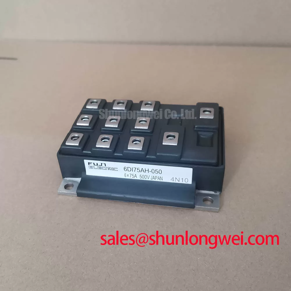
Benchtop Waveform Tuning: Mitigating Stress via High Frequency Commutation Loop Inductance on 6DI75B-050
For a heavy duty variable frequency AC motor drive, inspect the commutation loop before changing switching parameters. The collector voltage peak is governed by the DC link voltage plus the inductive overshoot created by stray loop inductance and current slew rate. This relationship makes busbar geometry, capacitor placement, and measurement technique as important as the transistor rating itself.
Design Consideration: Keep the high current path compact and symmetrical, place the local DC link capacitor close to the switching terminals, and avoid routing gate or feedback conductors beside the commutation loop. The required parasitic inductance target, snubber capacitance, and switching rate must be established by the system designer from measured waveforms rather than assumed from the module rating. Use a properly compensated differential probe and verify the probe loop does not create a false spike.
When a waveform shows excessive ringing, compare the collector to emitter voltage at the module terminals and at the DC link capacitor. A difference between these points may indicate busbar inductance, capacitor connection impedance, or probing error. Snubber selection should be validated for pulse energy, temperature rise, and repetitive duty. The Fuji Electric Power Semiconductors Portal is an appropriate manufacturer resource for confirming the applicable power semiconductor documentation.
| Parameter | Official Specification | Engineering Value Interpretation |
|---|---|---|
| Collector-Emitter Voltage, VCES | 500 V | One voltage parameter to evaluate for rectified 200 to 240 V AC line applications; complete suitability also depends on transient and operating conditions |
| Rated Collector Current, IC | 75 A | Rated current under the specified conditions; usable continuous current depends on temperature, switching operation, and thermal design |
| Peak Collector Current, ICP | 150 A | Specified short-duration current rating under its applicable datasheet conditions |
| Collector Power Dissipation, PC | 350 W | Specified power-dissipation rating; usable power depends on case temperature and the mounting and heatsink path |
| Operating Junction Temperature, Tj | −40°C to +150°C | Specified junction-temperature range for the device |
| Isolation Voltage, Visol | 2500 V AC for 1 minute | Isolation reference between the module terminals and its baseplate under the specified test conditions |
Transient Dynamics & Electrical Design: Gate Control and Miller Immunity on 6DI75B-050
High dv/dt in a bridge leg can couple through the device capacitances and disturb the opposing gate. For this reason, the gate driver should be evaluated as part of the complete switching loop, not as an isolated accessory. Confirm the actual gate terminal reference, driver return path, dead time, and turn off behavior from the original circuit documentation.
Negative gate bias and active Miller clamping are system level design options, not published operating requirements for this product page. If either technique is considered, the designer should verify the allowed gate voltage, driver supply limits, isolation arrangement, and transient response against the applicable Fuji Electric data. A low impedance gate loop with separated power and control returns can reduce unwanted turn on, while oscilloscope testing should confirm that the opposing switch remains safely off.
Thermal assessment must include switching loss, conduction loss, ambient temperature, heatsink performance, and airflow. The official 350 W collector power dissipation value should not be treated as an automatic operating allowance because the permitted power depends on case temperature and the thermal path. During commissioning, record case temperature and switching waveforms at the intended load rather than relying only on nominal current.
Transient Dynamics & Electrical Design: Braking Resistors and Chopper Transistor Evaluation
During motor deceleration, regenerated energy can raise the DC link voltage beyond the normal motoring condition. A braking chopper using an appropriately rated switching device and resistor must be evaluated for pulse energy, repetition rate, resistor cooling, and DC link control strategy. The 500 V VCES rating provides a device boundary, but it does not replace verification of the complete transient voltage at the collector and emitter terminals.
When replacing a failed module in a drive, inspect the braking resistor, DC link capacitors, gate driver output, current feedback, and any clamp network before installing the replacement. A new power transistor can be exposed to the same fault if the original overvoltage or gate control condition remains. For a neutral compatibility review, engineers may also compare the electrical and mechanical requirements of 7MBR15PE120, without treating it as an automatic substitute for the 6DI75B-050.
Long motor cables can behave as transmission lines and produce reflected voltage at the motor terminals. The drive designer should evaluate cable length, motor insulation, output filtering, switching edge rate, and measured peak voltage together. Do not assign a fixed filter value without checking the actual topology. Separate high current terminals from sensitive control wiring, maintain the required creepage and clearance for the working voltage, and follow the heatsink manufacturer’s instructions for TIM application and fastener torque.
Field Diagnostics & Commissioning: Reliability Limits in 6DI75B-050 Topologies
Reliability calculations involving FIT, terrestrial neutron flux, cosmic radiation, single event burnout, or altitude derating require qualified device data and a defined operating profile. No FIT rate or SEB probability should be assigned to this module from its voltage rating alone. At installations above 2000 m, the system engineer should verify the applicable insulation, cooling, and voltage derating requirements using the equipment standard, enclosure design, and manufacturer documentation.
For field diagnostics, isolate the drive, discharge the DC link according to the service procedure, and compare the suspected module with a known good signal path. Check terminal insulation, gate to emitter behavior, phase symmetry, driver supply stability, and the presence of abnormal collector voltage overshoot. Static multimeter diode mode readings can help identify an open or shorted power path, but they are not a complete dynamic health test.
Bench Tip: Use ESD protection and compare cold measurements taken at the same temperature, test instrument, and lead configuration before interpreting any difference.
Document the incoming condition, mounting surface, thermal interface, terminal connections, and first powered waveform. The Field Engineer’s Handbook provides a useful technical reference for structured testing, failure analysis, and reliability review.