



Content last revised on September 23, 2026
Field Diagnostics & Commissioning: Baseplate Thermal Resistance in PK160F-80 Topologies
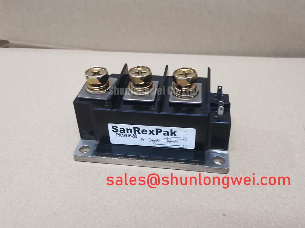
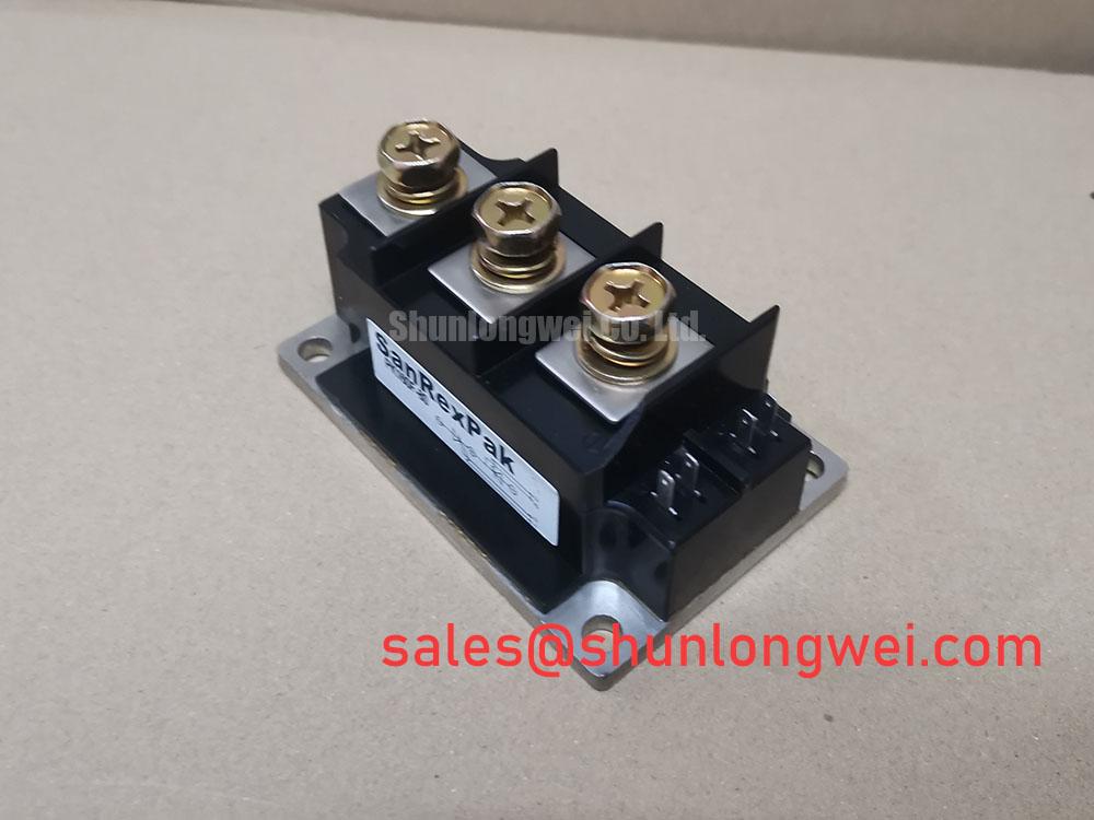
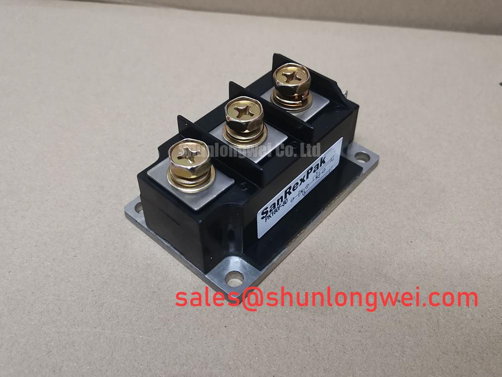
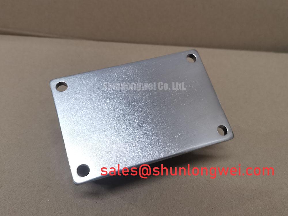
The insulated baseplate interface deserves inspection before the PK160F-80 is energized. Check that the heatsink surface is clean, flat, and free of embedded debris, oxidation, burrs, or old hardened interface residue. A damaged mounting plane can create uneven heat transfer even when electrical measurements appear acceptable. The 800 V and 160 A ratings are Official Datasheet Specifications, while the allowable junction temperature, junction to case thermal resistance, and mounting hardware requirements should be taken only from the applicable SanRex documentation for the exact package revision.
Thermal resistance across the baseplate is not usefully judged from a single external temperature reading. During controlled commissioning, compare temperature distribution across the heatsink, review load waveform conditions, and investigate local hot regions together with conductor condition and cooling flow. Uneven thermal paste spreading, warped heatsinks, or uneven clamping force may contribute to an abnormal thermal pattern. This is a Design Consideration rather than a PK160F-80 factory guarantee.
If the original equipment documentation specifies a fuse coordination table or I²t requirement, retain that coordination during service. Do not substitute a fuse by current rating alone, because semiconductor protection behavior depends on the complete fault path, prospective current, and clearing characteristic. Terminal screws should be tightened using the module documentation and equipment assembly requirement rather than a generic torque value.
💡 Bench Tip: Apply ESD precautions and capture cold terminal readings before installation so later checks can be compared with an unchanged baseline rather than memory.
For broader heat path evaluation, the practical discussion in The Advanced Thermal Management Revolution can help maintenance teams frame heatsink contact, interface material condition, and cooling verification without treating those general practices as model specific ratings.
Transient Dynamics & Electrical Design: Dynamic Voltage Sharing and RC Damping in PK160F-80
In thyristor and diode module assemblies, transient behavior must be assessed at the assembled circuit level. The PK160F-80 carries Official Datasheet ratings of 800 V and 160 A, but those figures do not by themselves define an RC snubber value, a saturable reactor requirement, or a firing network setting. Designers should examine the actual supply waveform, commutation path, cable routing, capacitor bank layout, and device voltage waveform during switching tests.
RC damping is a Design Consideration used where a measured transient or ringing condition requires controlled energy dissipation and a reduced rate of voltage change. The resistor and capacitor must be evaluated as a pair, including repetitive pulse stress and heat dissipation. Likewise, a series reactor can influence current rise and current sharing, but its selection remains system determined. The integration objective is to minimize parasitic loop inductance where it can create overshoot, then verify peak device stress against the measured DC link or line related voltage in the finished assembly.
For a grid tied static var compensator or thyristor switched capacitor installation, inspect gate drive return routing and reference connections together with the main power loop. Spurious triggering may arise from several conditions, including coupling between high energy conductors, incorrect gate circuit connections, timing issues, or a damaged driver stage. Use an isolated measurement method appropriate to the system voltage and compare waveforms with the documented control sequence.
A front end or auxiliary rectifier stage may use a separate module such as PD104SL7, subject to independent verification of circuit topology, pinout, electrical ratings, and mechanical compatibility. The manufacturer context for power semiconductor module families can also be reviewed at SanRex Sansha Electric Power Semiconductors.
Assembly Integrity & Layout Architecture: Implementing Dynamic Firing Delay Angle Adjustment for PK160F-80
Before adjusting firing delay angle in a controlled rectifier or capacitor switching arrangement, verify that every gate and power terminal corresponds to the host schematic. The PK160F-80 designation, its 800 V rating, its 160 A rating, and its isolated power module form factor identify the unit, but they do not establish gate lead assignments or internal device arrangement without the correct manufacturer drawing. Never infer terminal identity from enclosure appearance alone.
Across a firing angle range from zero to 150 degrees, the resulting AC to DC transfer behavior depends on the complete converter topology, source impedance, load characteristics, commutation conditions, and control strategy. As firing is delayed, the system can experience changed real power transfer, altered displacement power factor, and different reactive power demand. These are circuit principles, not fixed PK160F-80 performance values. When integrating the module into static var compensation equipment, system engineers should validate timing with the original controller logic and confirm synchronization under representative line conditions.
Layout work should keep gate related wiring clearly separated from high energy power conductors where practical, while maintaining the intended return path defined by the equipment design. Check for loose lugs, signs of heat at terminal interfaces, damaged insulation sleeves, and cable strain transmitted into the module terminals. After assembly, controlled low energy verification of the trigger sequence can expose a wiring or timing discrepancy before full system duty is applied.
Where a cross reference is being evaluated for an existing assembly, PD104VT2T1 is a related power semiconductor listing that can be reviewed as an objective comparison point. Its electrical, mechanical, terminal, thermal, and control characteristics must be checked separately; it should not be treated as an automatic replacement for PK160F-80.
PK160F-80 Circuit Protection & Reliability: Calibrating Sinusoidal 10ms Half Cycle Surge Current Limits
Do not assign a sinusoidal 10 ms half cycle surge current value to the PK160F-80 unless it is taken directly from the applicable official datasheet. The confirmed official identification data are 800 V, 160 A, and isolated power module. Surge current capability, I²t limits, repetitive overload conditions, reverse voltage reapplication limits, and allowable junction temperature boundaries require the model specific manufacturer table.
After a fault event, begin with a safe isolation procedure and inspect the protection chain as a complete system. Examine semiconductor fuses, contactors, busbars, snubber components, capacitor bank connections, and control timing records where available. A failed protection component can be the result of an upstream transient, a connection issue, an application fault, or an incorrectly coordinated protective device. Static diode mode checks can identify certain gross junction failures, while controlled dynamic testing is needed to assess switching and blocking behavior.
Reliability assessment should remain evidence based. No field lifetime, failure rate, altitude derating, cosmic ray susceptibility, insulation reliability, EMC compliance, or safety certification claim is assigned here because no applicable model specific source has been provided. As a Design Consideration, engineers evaluating severe electrical or thermal duty should use the original equipment validation procedure and relevant manufacturer documentation. For an additional industry reference on power semiconductor module categories, consult Shindengen Power Semiconductor Modules and Diodes.